Selection of epitaxial growth strain measurement method and quantum well laser fabrication method and quantum well laser
A technology for selecting epitaxy and strain measurement, applied in the field of information optoelectronics, it can solve the problems of affecting laser performance, inaccurate measurement, expensive and other problems, and achieve the effect of avoiding material defects, good performance and low cost
- Summary
- Abstract
- Description
- Claims
- Application Information
AI Technical Summary
Problems solved by technology
Method used
Image
Examples
Embodiment 1
[0031] This embodiment discloses a method for measuring the strain of selective epitaxial growth, including the following steps:
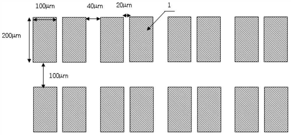
[0032] 1) Forming SiO on a semiconductor material substrate 2 Mask 1, select the epitaxial growth material on the substrate with the mask;
[0033] 2) All the epitaxial materials except the selected epitaxial growth area 2 are removed by photolithography process, and the SiO2 mask material is removed, leaving only the material of the selected epitaxial growth area;
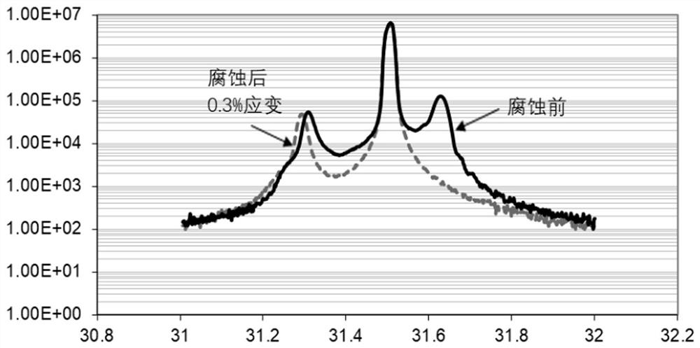
[0034] 3) The strain is measured by X-ray diffractometer, because the material outside the selected epitaxial region has been completely removed, so the measured strain is the strain of the material in the selected epitaxial region. This method does not need to use expensive micro-region X-ray diffraction equipment to measure the strain of the selected epitaxial growth region, thus providing a low-cost and accurate method for the characterization of the selected epitaxial growth mater...
Embodiment 2
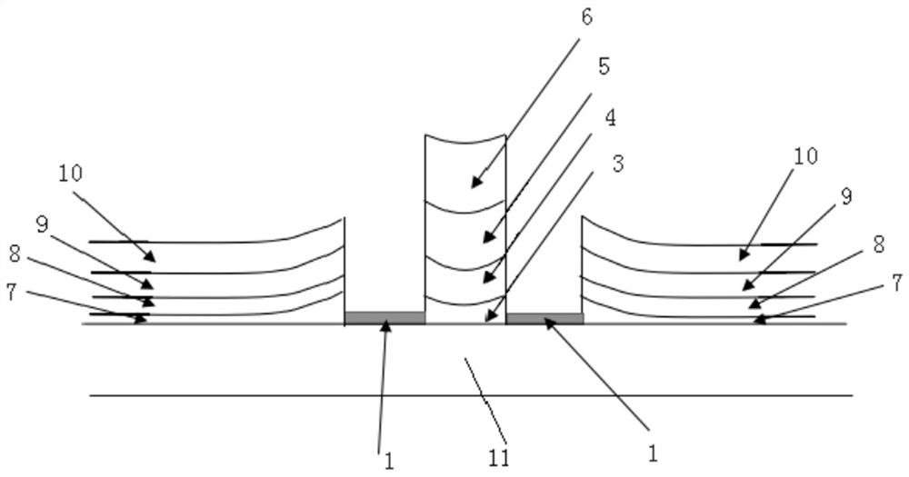
[0042] see Figure 4 , the present embodiment discloses a selective epitaxial growth quantum well laser manufacturing method, comprising the following steps:
[0043] 1) Use the selective epitaxial growth strain measurement method disclosed in Example 1 to measure the strain of the material of the lower waveguide layer, which is set to ε;
[0044] 2) Form SiO on the semiconductor substrate 2 mask, such as Figure 4 As shown in 1, each epitaxial layer is sequentially grown on the semiconductor substrate as required, such as on an InP substrate, an InP buffer layer, a lower waveguide layer, a quantum well layer, and an upper waveguide layer are grown sequentially, such as Figure 4 The shown buffer layer 3 , lower waveguide layer 4 , quantum well layer 5 , upper waveguide layer 6 and buffer layer 7 , lower waveguide layer 8 , quantum well layer 9 , and upper waveguide layer 10 .
[0045] Growing the lower waveguide layer specifically includes: growing a strain-compensated low...
PUM
 Abstract
Description
Claims
Application Information


