Method for manufacturing MOS device

A technology of MOS devices and manufacturing methods, which is applied in the manufacturing of semiconductor/solid-state devices, semiconductor devices, electrical components, etc., can solve the problems that the effect cannot reach the expected effect, and the requirements of the process cannot be met.

Active Publication Date: 2020-03-06
SHANGHAI HUALI MICROELECTRONICS CORP
View PDF5 Cites 0 Cited by
  • Summary
  • Abstract
  • Description
  • Claims
  • Application Information

AI Technical Summary

Problems solved by technology

Its effect can not achieve the expected effect

Method used


Image

  • Method for manufacturing MOS device
  • Method for manufacturing MOS device
  • Method for manufacturing MOS device

Examples


Embodiment Construction

[0028] The manufacturing method of the MOS device proposed by the present invention will be further described in detail below with reference to the drawings and specific embodiments. The advantages and features of the present invention will become clearer from the following description. It should be noted that all the drawings are in a very simplified form and use imprecise scales, and are only used to facilitate and clearly assist the purpose of illustrating the embodiments of the present invention.

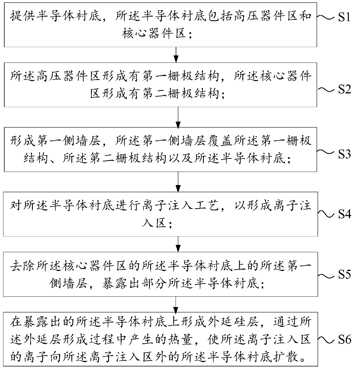
[0029] Please refer to figure 1 , figure 1 It is a flowchart of a method for manufacturing a MOS device provided by an embodiment of the present invention;

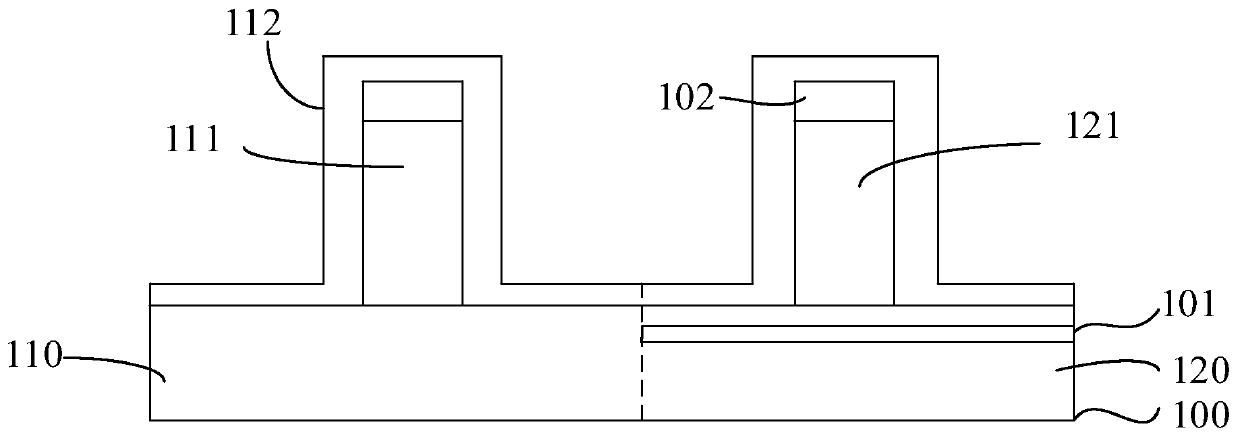
[0030] Step S1: providing a semiconductor substrate, the semiconductor substrate including a high-voltage device region and a core device region;

[0031] Step S2: a first gate structure is formed in the high-voltage device region, and a second gate structure is formed in the core device region;

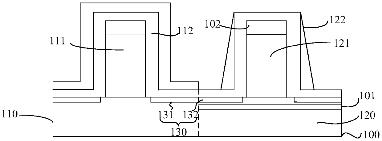
[0032] Step S3: formin...


PUM

PropertyMeasurementUnit
Thicknessaaaaaaaaaa

Abstract

A method for manufacturing a MOS device provided by the present invention comprises: forming a first spacer layer covering a first gate structure, a second gate structure, and a semiconductor substrate; performing an ion implantation process on the semiconductor substrate to form an ion implantation region; removing the first spacer layer on the semiconductor substrate in a core device region to expose a portion of the semiconductor substrate; forming an epitaxial silicon layer on the exposed semiconductor substrate, wherein heat is generated during the growth of the epitaxial silicon layer, and ions in the ion implantation region can diffuse to the semiconductor substrate outside the ion implantation region. Thus, the method can replace an annealing process to suppress a hot carrier injection effect and improve the performance of the device. In addition, since a subsequent annealing process is eliminated, processing time can be saved.

Description

technical field [0001] The invention relates to the technical field of semiconductor manufacturing, in particular to a method for manufacturing a MOS device Background technique [0002] MOS (Metal Oxide Semiconductor) devices are well known in the art, and the HCI (Hot Carrier Injection) effect in the manufacturing process of MOS devices will cause performance degradation of MOS devices and affect the reliability of MOS devices. For semiconductor devices, when the feature size of the device is small, a strong electric field can be generated even at a low voltage, which easily leads to the occurrence of hot carriers. Therefore, in small-scale devices and large-scale integrated circuits, hot carriers are prone to appear. [0003] At present, in order to improve the HCI effect of MOS devices, the industry usually adopts the optimization method of lightly doped source / drain implantation (LDD) ion implantation. By reducing the dose of LDD ion implantation and increasing the ene...

Claims


Application Information

Patent Timeline
IPC IPC(8): H01L21/8234H01L27/088H01L29/06
CPCH01L21/8234H01L27/088H01L29/0684
Inventor 汪韬唐小亮
Owner SHANGHAI HUALI MICROELECTRONICS CORP
Why Eureka
Try Eureka