
Optical element, liquid crystal display device, and projection-type image display device

A technology of optical elements and compensating elements, which is applied in the direction of optical elements, optical elements, optics, etc., can solve the problems of insufficient space for configuring polarizing plates or phase difference compensation plates, problems in durability, and difficulty in adapting to miniaturization, etc., and achieve high suppression Effects of reducing costs, realizing reductions, and reducing adjustment man-hours

Active Publication Date: 2020-03-17
DEXERIALS CORP
View PDF9 Cites 0 Cited by
  • Summary
  • Abstract
  • Description
  • Claims
  • Application Information

AI Technical Summary

Problems solved by technology

[0006] However, in recent years, liquid crystal display devices have continued to be miniaturized, and the space for arranging polarizing plates or retardation compensation plates has gradually become insufficient.
Therefore, in the optical compensation method described in Patent Document 2, since two phase difference compensation plates and a rotation mechanism for rotating the two phase difference compensation plates are required, there is a concern that the mounting space will increase and it will be difficult to adapt to miniaturization.
[0007] In addition, since the retardation compensation plate described in Patent Document 3 is formed by laminating two compensation layers, an adhesive is required, and there is a problem in durability.
In addition, since two substrates are required, there is a concern about cost increase

Method used


Image

  • Optical element, liquid crystal display device, and projection-type image display device
  • Optical element, liquid crystal display device, and projection-type image display device
  • Optical element, liquid crystal display device, and projection-type image display device

Examples


preparation example Construction

[0107] [Preparation method of polarizer]

[0108] The polarizer constituting the optical element of the present invention can be produced by going through a metal film forming step, a first dielectric film forming step, an absorbing film forming step, and an etching step.

[0109] In the metal film forming step, a metal film that becomes a linear metal layer in a subsequent etching step is formed on the entire substrate surface on one side of the transparent substrate. In the first dielectric film forming step, the first dielectric film that becomes the first dielectric layer through the subsequent etching step is laminated on the entire surface of the metal film formed in the metal film forming step. In the absorbing film forming step, an absorbing film to be an absorbing layer through the subsequent etching step is laminated on the entire surface of the first dielectric film formed in the first dielectric film forming step. In these respective formation steps, various films...

Embodiment 1

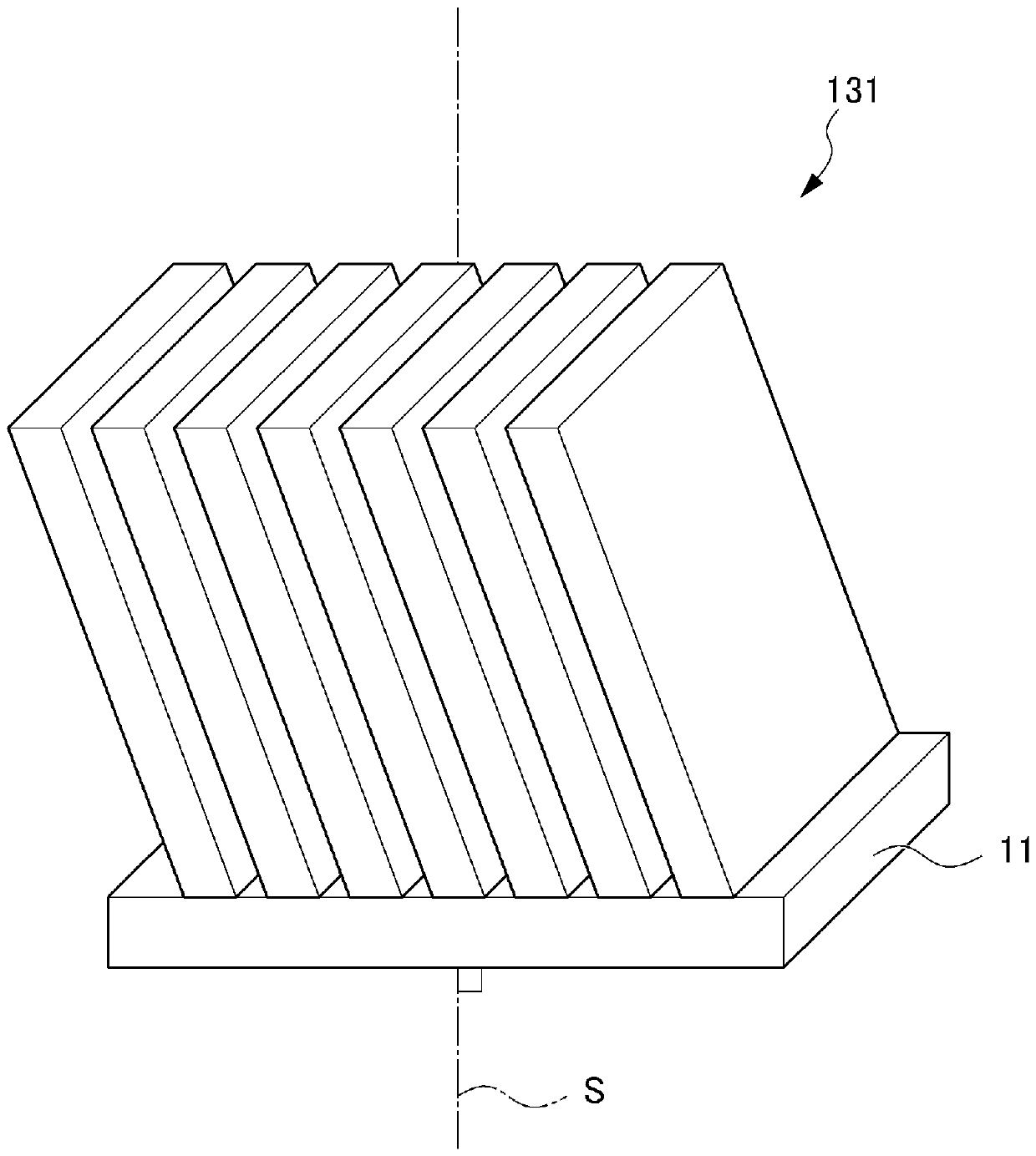
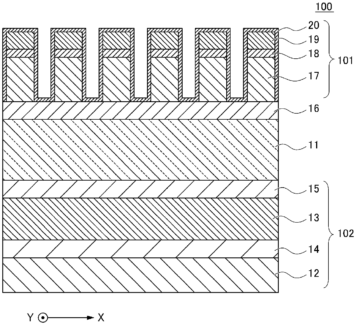
[0155] In Example 1, making figure 1 Optical elements of the composition shown.

[0156] [Production of polarizer]

[0157] (Formation of the third dielectric layer)

[0158] On one side of the glass substrate (average thickness 0.7 mm), SiO 2 Film formation, thereby forming the third dielectric layer ( figure 1 The third dielectric layer 16).

[0159] (formation of metal film)

[0160] Next, an Al film was formed on the third dielectric layer by a sputtering method to form a metal film.

[0161] (Formation of the first dielectric film)

[0162] Next, on the metal film, the SiO 2 The film is formed to form a first dielectric film.

[0163] (formation of absorbing film)

[0164] Next, Si is formed into a film by sputtering on the first dielectric film to form an absorption film.

[0165] (Formation of grid-like protrusions)

[0166] Next, a resist is applied on the absorbing film, followed by exposure and development to form a resist pattern. Then, etching is perfor...


PUM

PropertyMeasurementUnit
refractive indexaaaaaaaaaa

Abstract

The invention relates to an optical element, a liquid crystal display device, and a projection-type image display device, which significantly reduce arrangement space, have superior durability, and also enable increased costs to be curbed. Functions of a polarizer and a phase difference compensation element are integrated. Specifically, the optical element provided has a transparent substrate, anda polarizer on one side of the transparent substrate, and has a phase difference compensation element on a side of the transparent substrate opposite from the polarizer.

Description

technical field [0001] The present invention relates to an optical element, a liquid crystal display device and a projection type image display device. Background technique [0002] In a liquid crystal display device, it is necessary to arrange a polarizing plate (polarizing plate) on a liquid crystal panel because of the principle of image formation. In addition, in liquid crystal display devices, in order to improve contrast and viewing angle characteristics, an optical compensation technique using a retardation compensation plate is used. [0003] As a polarizing plate used in a liquid crystal display device, for example, an absorption-type wire-grid polarizing plate has been proposed in which metal lattices at a pitch smaller than the wavelength of light in the use frequency band (use band) are formed on a substrate, and A dielectric layer and an inorganic fine particle layer are formed on the metal grid, and while canceling light reflected from the metal grid by the in...

Claims


Application Information

Patent Timeline
Patent Type & Authority Applications(China)
IPC IPC(8): G02B5/30G02F1/1335G02F1/13363G03B21/00
CPCG02B5/3016G02B5/3058G02F1/133528G02F1/133632G03B21/006G02F2413/02G02F1/133634G02F1/136277G02F2413/07G02F2413/03G02F2413/105G02F1/133531G02F1/13712B29D11/00644B29D11/0073G02B1/115G02F1/133548G02F1/13363G02B1/118G02B5/3008
Inventor 菅原淳一
Owner DEXERIALS CORP
Learn More