OLED display panel and manufacturing method thereof

A technology for display panels and manufacturing methods, which is applied in semiconductor/solid-state device manufacturing, electrical components, electrical solid-state devices, etc., can solve problems such as the complexity of the isolation column manufacturing process, achieve optimized panel display effects, optimize process structures, and save costs. Effect

Active Publication Date: 2020-03-24
SHENZHEN CHINA STAR OPTOELECTRONICS SEMICON DISPLAY TECH CO LTD
View PDF22 Cites 28 Cited by
  • Summary
  • Abstract
  • Description
  • Claims
  • Application Information

AI Technical Summary

Problems solved by technology

Solve the problem that the manufacturing process of the isolation column is complicated in the prior art

Method used


Image

  • OLED display panel and manufacturing method thereof
  • OLED display panel and manufacturing method thereof
  • OLED display panel and manufacturing method thereof

Examples


Embodiment Construction

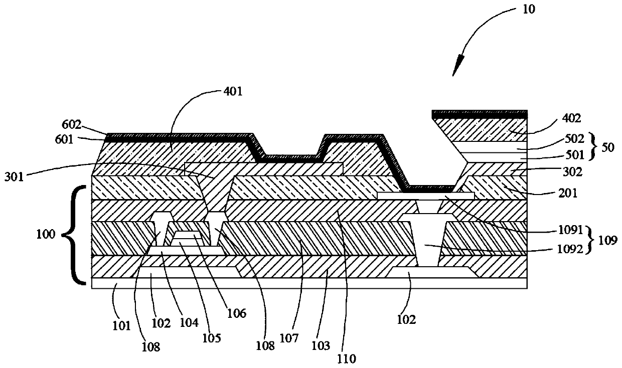
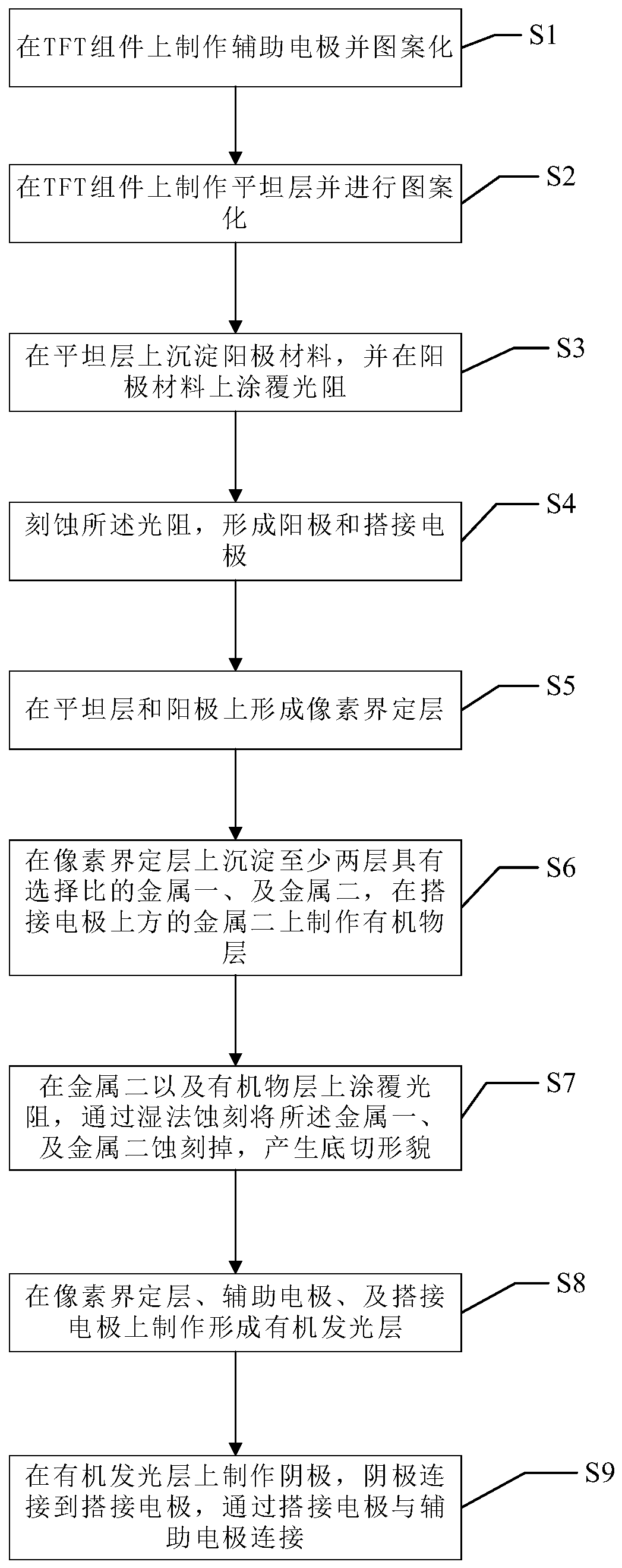
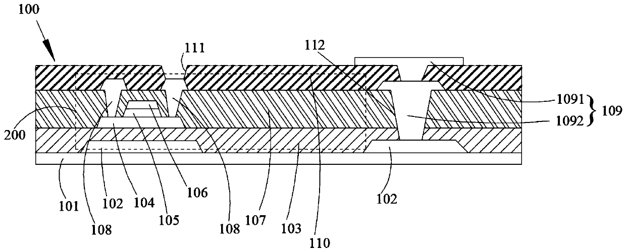
[0042] The technical solutions in the embodiments of the present application will be clearly and completely described below in conjunction with the drawings in the embodiments of the present application. Apparently, the described embodiments are only some of the embodiments of this application, not all of them. Based on the embodiments in this application, all other embodiments obtained by those skilled in the art without making creative efforts belong to the scope of protection of this application.

[0043]In the description of the present application, it should be understood that the terms "center", "longitudinal", "transverse", "length", "width", "thickness", "upper", "lower", "front", " Orientation indicated by rear, left, right, vertical, horizontal, top, bottom, inside, outside, clockwise, counterclockwise, etc. The positional relationship is based on the orientation or positional relationship shown in the drawings, which is only for the convenience of describing the ap...


PUM


Abstract

The invention provides an OLED display panel and a manufacturing method thereof. The OLED display panel comprises a TFT assembly, an auxiliary electrode, an anode, a lap joint electrode, a metal layer, an organic matter layer, an organic light-emitting layer and a cathode. The lap joint electrode is connected with the auxiliary electrode, and the organic light-emitting layer and the cathode are connected with the auxiliary electrode; and the metal layer and the organic matter layer have undercut structures.

Description

technical field [0001] The invention relates to the field of display technology, in particular to an OLED display panel and a manufacturing method thereof. Background technique [0002] Display panels, such as Organic Light-Emitting Diode (OLED for short), have attracted great attention from academia and industry because of their great development potential in the direction of solid-state lighting and flat panel display. OLED has many advantages such as self-illumination, low driving voltage, high luminous efficiency, short response time, high definition and contrast, nearly 180° viewing angle, wide temperature range, flexible display and large-area full-color display, etc., and is recognized by the industry. It is the display device with the most development potential. [0003] Large-sized OLED panels will produce different IR voltage drops (IR Drop) at different positions due to the large resistance of the cathode during operation, resulting in uneven brightness of the OL...

Claims


Application Information

Patent Timeline
Patent Type & Authority Applications(China)
IPC IPC(8): H01L27/32H01L51/52
CPCH10K59/12H10K50/814H10K50/824H10K59/1201
Inventor 张良芬
Owner SHENZHEN CHINA STAR OPTOELECTRONICS SEMICON DISPLAY TECH CO LTD
Why Eureka
Try Eureka