Thin film transistor array substrate, preparation method for same and display device of thin film transistor array substrate

A technology of thin film transistors and array substrates, which is applied in the field of liquid crystal display, can solve the problems of complex manufacturing process of thin film transistor array substrates, and achieve the effect of simplifying the manufacturing process

Inactive Publication Date: 2014-04-30
BEIJING BOE OPTOELECTRONCIS TECH CO LTD +1
View PDF5 Cites 0 Cited by
  • Summary
  • Abstract
  • Description
  • Claims
  • Application Information

AI Technical Summary

Problems solved by technology

[0006] Embodiments of the present invention provide a thin film transistor array substrate, a manufacturing method thereof, and a display device, which are used to solve the problem of complex manufacturing process of the existing thin film transistor array substrate

Method used


Image

  • Thin film transistor array substrate, preparation method for same and display device of thin film transistor array substrate
  • Thin film transistor array substrate, preparation method for same and display device of thin film transistor array substrate
  • Thin film transistor array substrate, preparation method for same and display device of thin film transistor array substrate

Examples


preparation example Construction

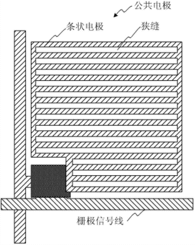
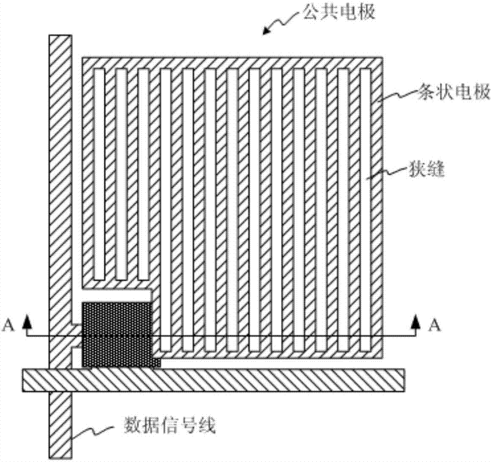
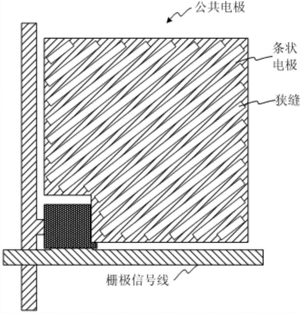
[0045] Based on the same inventive concept, an embodiment of the present invention also provides a method for preparing a thin film transistor array substrate, in which the preparation of the common electrode includes:

[0046] The pattern of the common electrode with a slit-like structure is formed through a patterning process, wherein the strip-shaped electrodes in the common electrode can reflect the light incident on the strip-shaped electrode, and the slits in the common electrode can transmit the light incident on the strip-shaped electrode. Slits of light.

Embodiment 1

[0048] Embodiment one, see Figure 2A ~ Figure 2G As shown, among them, Figure 2A ~ Figure 2G for Figure 1B In the schematic diagram of the cross-sectional structure in the direction of A-A, the manufacturing process of this embodiment includes the following steps:

[0049] (1) Form the gate 2 on the base substrate 1, such as Figure 2A shown;

[0050] Specifically, a metal layer (such as molybdenum Mo, aluminum Al, etc.) is deposited on a substrate (such as a glass substrate), and a gate pattern is formed by wet etching through the first photolithography technology.

[0051] (2) Forming the gate insulating layer 3 and the active layer 4 on the substrate on which the gate 2 is formed, such as Figure 2B shown;

[0052] Specifically, a gate insulating layer (Gate Insulator, GI) film and an oxide semiconductor film (such as Indium Gallium Zinc Oxide (IGZO) etc.) Secondary photolithography technology, wet etching to form the pattern of the active layer (pattern);

[0053...

Embodiment 2

[0067] Embodiment two, see Figure 3A ~ Figure 3F As shown, among them, Figure 3A ~ Figure 3F for Figure 1B In the schematic diagram of the cross-sectional structure in the direction of A-A, the manufacturing process of this embodiment includes the following steps:

[0068] (1) The gate 2 is formed on the base substrate 1, such as Figure 3A shown;

[0069] Specifically, a metal layer (such as molybdenum Mo, aluminum Al, etc.) is deposited on a substrate (such as a glass substrate), and a gate pattern is formed by wet etching through the first photolithography technology.

[0070] (2) Forming a gate insulating layer 3, an active layer 4, and an etch stop layer 5 on the substrate on which the gate 2 is formed, such as Figure 3B shown;

[0071] Specifically, the GI layer film, the oxide semiconductor film and the etch stop layer film are continuously deposited on the base substrate on which the gate is formed, and the pattern of the etch stop layer is formed by dry etchi...


PUM


Abstract

The invention discloses a thin film transistor array substrate, a preparation method for the same and a display device of the thin film transistor array substrate. The problem that the manufacturing process of the existing thin film transistor array substrate is complicated is solved. According to an embodiment of the invention, the thin film transistor array substrate comprises a plurality of pixel units, wherein each pixel unit comprises a common electrode; patterns of the common electrodes are slit-shaped; each common electrode comprises a strip-shaped electrode and a slit; the strip-shaped electrode in each common electrode can reflect light rays emitted in the strip-shaped electrode; and the slit in each common electrode can transmit light rays emitted in the slit. By using the thin film transistor array substrate, the strip-shaped electrodes in the common electrodes can serve as reflecting areas of the array substrate, and the slits of the common electrodes can serve as transmitting areas of the array substrate, so that the semi-transmitting and semi-reflecting characteristic is realized. Because the slit-shaped common electrodes can be manufactured by using a mask process, the manufacturing process is simplified.

Description

technical field [0001] The present invention relates to the technical field of liquid crystal display, in particular to a thin film transistor array substrate, a preparation method thereof, and a display device including the above thin film transistor array substrate. Background technique [0002] Liquid Crystal Display Panel (LCD, Liquid Crystal Display Panel) has the characteristics of low power consumption, low radiation and low manufacturing cost, and has been widely used in various electronic equipment, such as digital electronic equipment such as display devices, TVs, mobile phones, and digital cameras. . Liquid crystal display panels are passive light-emitting devices, which can be divided into reflective, transmissive, and transflective types according to the light source. [0003] The reflective liquid crystal display panel uses the ambient light around the liquid crystal display panel as the light source, and the reflective liquid crystal display panel is provided...

Claims


Application Information

Patent Timeline
IPC IPC(8): G02F1/1343G02F1/1362G02F1/1368H01L27/12H01L23/50H01L21/84
CPCG02F1/133555G02F1/134363H01L27/1259G02F1/134318H01L21/84H01L27/12H01L27/124H01L27/1262
Inventor 张家祥郭建姜晓辉阎长江
Owner BEIJING BOE OPTOELECTRONCIS TECH CO LTD
Why Eureka
Try Eureka