Organic light-emitting diode display panel and preparation method thereof

A technology for light-emitting diodes and display panels, which is used in semiconductor/solid-state device manufacturing, electrical components, and electrical solid-state devices, etc., and can solve problems such as electrode instability.

Active Publication Date: 2020-03-24
SHENZHEN CHINA STAR OPTOELECTRONICS SEMICON DISPLAY TECH CO LTD
View PDF15 Cites 4 Cited by
  • Summary
  • Abstract
  • Description
  • Claims
  • Application Information

AI Technical Summary

Problems solved by technology

However, electrodes such as Ba

Method used


Image

  • Organic light-emitting diode display panel and preparation method thereof
  • Organic light-emitting diode display panel and preparation method thereof
  • Organic light-emitting diode display panel and preparation method thereof

Examples


Embodiment Construction

[0023] In order to make the above-mentioned and other objects, features, and advantages of the present disclosure more clearly understood, the preferred embodiments of the present disclosure will be exemplified below, and will be described in detail in conjunction with the accompanying drawings. Furthermore, the directional terms mentioned in the present disclosure, such as upper, lower, top, bottom, front, rear, left, right, inner, outer, lateral, peripheral, central, horizontal, lateral, vertical, longitudinal, axial , radial, uppermost or lowermost, etc., only refer to the directions of the attached drawings. Accordingly, the directional terms used are used to describe and understand the present disclosure, rather than to limit the present disclosure.

[0024] In the figures, structurally similar elements are denoted by the same reference numerals.

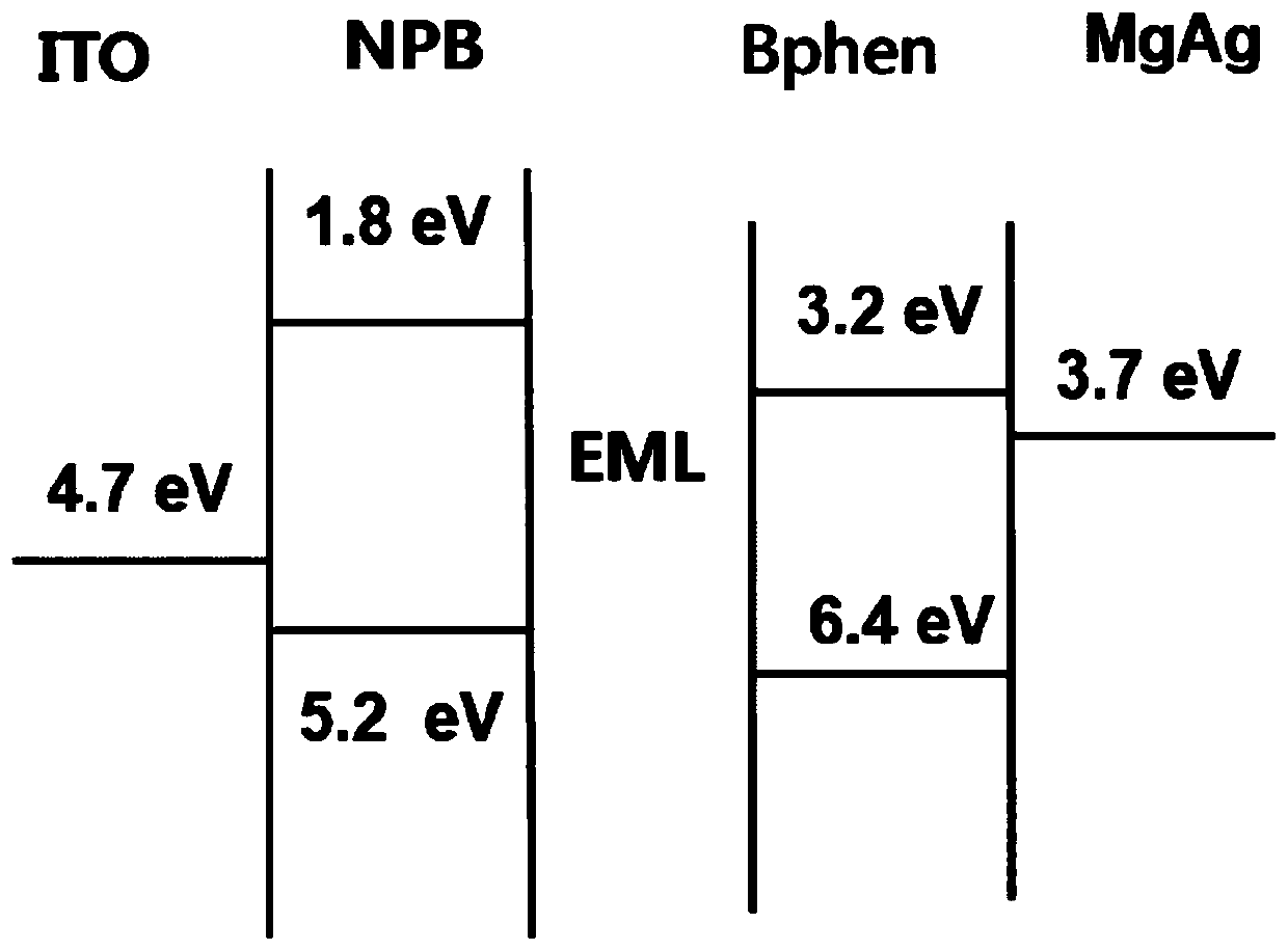
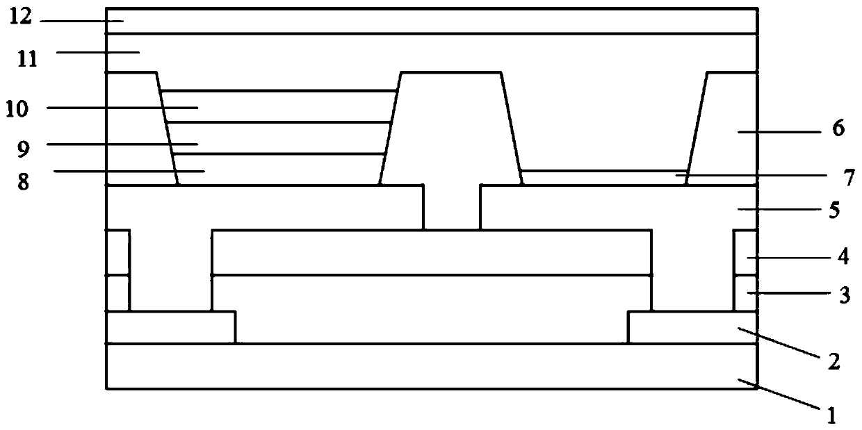
[0025] figure 2 A schematic diagram of the structure of the organic light emitting diode display panel according to the pr...


PUM


Abstract

The invention discloses an organic light-emitting diode display panel and a preparation method thereof. The organic light-emitting diode display panel includes: a backboard; the plurality of metal wiring layers are arranged on the backboard; the passivation layer is arranged on the metal wiring layer and the backboard; the planarization layer is arranged on the passivation layer; the plurality offirst electrode layers are arranged on the planarization layer and are electrically connected with the metal wiring layer through first via holes; the plurality of pixel definition layers are arrangedon the first electrode layer; wherein each two adjacent pixel definition layers are respectively defined with an organic light-emitting diode device region or an auxiliary cathode contact hole region, and the organic light-emitting diode device regions and the auxiliary cathode contact hole regions are arranged at intervals; the auxiliary cathode contact hole region includes an electrode modification layer disposed on the first electrode layer. By arranging the electrode modification layer, the voltage drop is reduced, and the brightness uniformity of the panel is improved.

Description

【Technical field】 [0001] The present disclosure relates to the field of display technology, and in particular, to an organic light emitting diode display panel and a manufacturing method thereof. 【Background technique】 [0002] A large-size Active-Matrix Organic Light-Emitting Diode (AMOLED) display adopts a top-emitting panel structure, which can fully improve the resolution of the panel. In the top-emitting AMOLED structure, the light emitted by the organic light emitting diode (OLED) with the device structure needs to pass through the electron transport layer and the cathode. Therefore, the electron transport layer and the cathode must have sufficient transparency, so the thinner the cathode, the better, but The reduction in the thickness of the cathode will inevitably increase the resistance of the cathode, and when the panel is operating, the current flowing through the high-resistance transparent cathode will cause a voltage drop in the center and around the large-size...

Claims


Application Information

Patent Timeline
IPC IPC(8): H01L51/52H01L27/32H01L21/77
CPCH10K59/122H10K50/81H10K50/824H10K59/1201
Inventor 陈金祥
Owner SHENZHEN CHINA STAR OPTOELECTRONICS SEMICON DISPLAY TECH CO LTD
Why Eureka
Try Eureka