PCB device welding method and device

A PCB board and welding method technology, applied in the field of devices and PCB board device welding methods, can solve problems such as poor welding of devices, achieve the effects of strengthening the output of good products, solving poor welding, and saving cost and resources

Inactive Publication Date: 2020-03-27
INSPUR SUZHOU INTELLIGENT TECH CO LTD
View PDF4 Cites 1 Cited by
  • Summary
  • Abstract
  • Description
  • Claims
  • Application Information

AI Technical Summary

Problems solved by technology

[0006] In view of this, the purpose of the present invention is to provide a method and device for soldering PCB components, which can effectively solve the problem of poor soldering of components, as well as maintenance costs, labor and other costs caused by poor

Method used


Image

  • PCB device welding method and device
  • PCB device welding method and device
  • PCB device welding method and device

Examples


Embodiment Construction

[0038] The following will clearly and completely describe the technical solutions in the embodiments of the present invention with reference to the accompanying drawings in the embodiments of the present invention. Obviously, the described embodiments are only some, not all, embodiments of the present invention. Based on the embodiments of the present invention, all other embodiments obtained by persons of ordinary skill in the art without making creative efforts belong to the protection scope of the present invention.

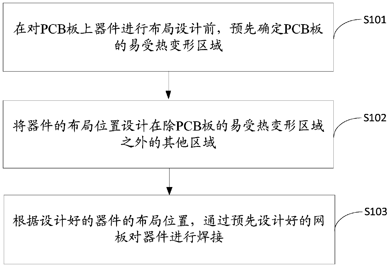
[0039] The invention provides a PCB board device welding method, such as figure 1 shown, including the following steps:

[0040] S101. Before performing layout design on the components on the PCB, predetermine the thermally deformable area of ​​the PCB;

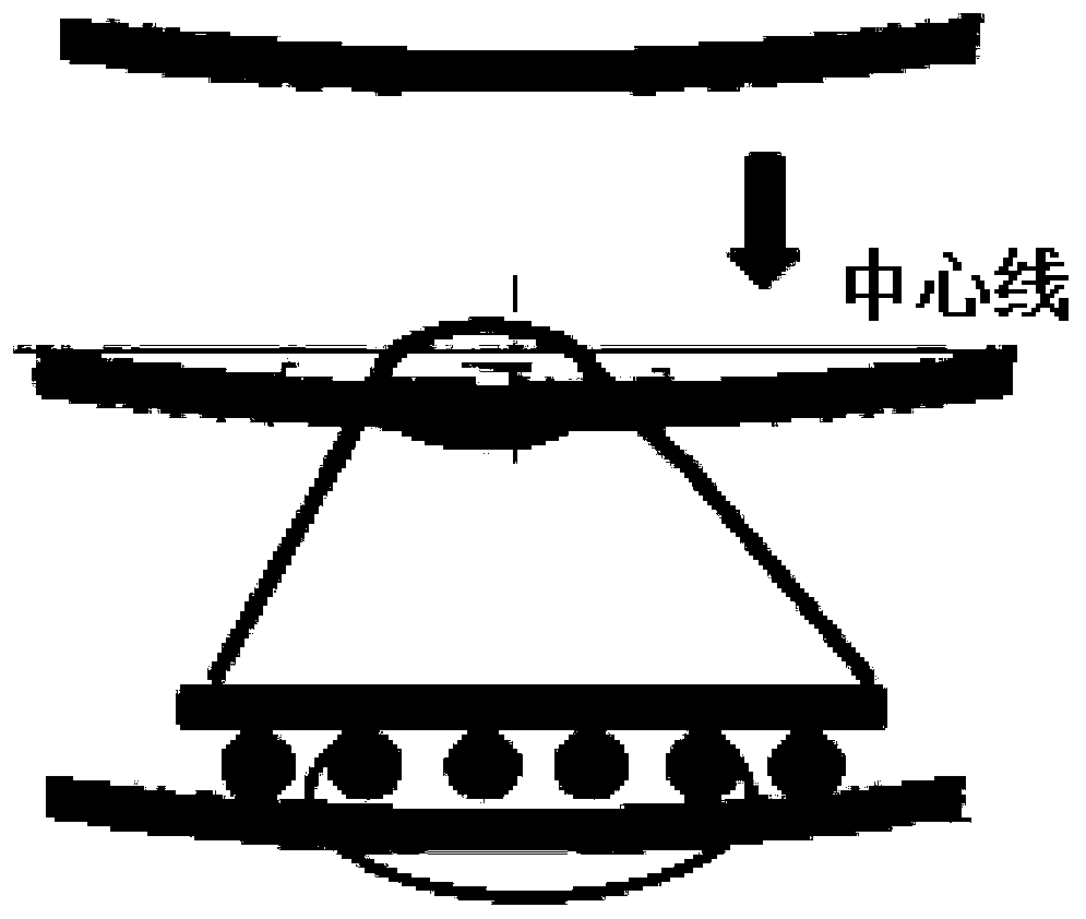
[0041] The analysis direction of the present invention is aimed at the layout of the device. Since the PCB is easily deformed by heat, the welding problem of the device should be reduced from the most fundam...


PUM


Abstract

The invention discloses a PCB device welding method and device, and the method comprises the steps of pre-determining an area easy to be heated and deformed, of a PCB before the layout design of the devices on the PCB; designing the layout positions of the devices in other areas except the area easy to be heated and deformed, of the PCB; and welding the devices through a pre-designed screen plateaccording to the designed layout positions of the devices. According to the present invention, firstly, by determining the area easy to be heated and deformed of the PCB before layout, keeping away the layout position of the devices from the area with the maximum deformation, and then welding after the reasonable layout is completed, so that the problem of poor device welding is effectively solved, and the maintenance cost, manpower cost and the like caused by the poor welding are effectively saved. the PCBA device welding method and device is suitable for all PCBA board cards with large device chips, a large number of cost resources can be saved, the yield of the good products is effectively enhanced, and therefore the productivity benefits and economic benefits are increased.

Description

technical field [0001] The invention relates to the technical field of PCB welding, in particular to a PCB device welding method and device. Background technique [0002] At present, the application of device ball grid array packaging chips is very common, and it is an indispensable chip in the electronics industry chain. It is a packaging method for integrated circuits using organic carrier boards. It has: 1. Small packaging area; 2. Increased function and increased number of pins; 3. Self-centering of printed circuit board (PCB) during soldering, easy to tin; 4. High reliability; 5. , Good electrical performance and so on. [0003] However, the problem that plagues the entire electronics industry now is the soldering of devices. In many electronic products, there are many cases of poor soldering of such devices, especially for devices with larger areas, the higher the rate of defective soldering. If the solder ball pin (Pin) of the device and the PCB PAD do not form an a...

Claims


Application Information

Patent Timeline
Patent Type & Authority Applications(China)
IPC IPC(8): H05K3/34
CPCH05K3/34
Inventor 张小行
Owner INSPUR SUZHOU INTELLIGENT TECH CO LTD
Why Eureka
Try Eureka