Printed circuit board and manufacturing method thereof and terminal

A technology of printed circuit boards and printed circuits, which is applied in the fields of printed circuit manufacturing, printed circuits, printed circuits, etc., can solve the problems of debugging radio frequency printed circuit boards, and achieve the effect of reducing the size of the area

Active Publication Date: 2020-04-10
SPREADTRUM COMM (SHANGHAI) CO LTD
View PDF3 Cites 2 Cited by
  • Summary
  • Abstract
  • Description
  • Claims
  • Application Information

AI Technical Summary

Problems solved by technology

Under this condition, it is difficult for small manufacturers with relatively weak technical capabilities to debug RF printed circuit boards that meet the needs of 5G communication through surface-mount RF PCBs.

Method used


Image

  • Printed circuit board and manufacturing method thereof and terminal
  • Printed circuit board and manufacturing method thereof and terminal
  • Printed circuit board and manufacturing method thereof and terminal

Examples


Embodiment Construction

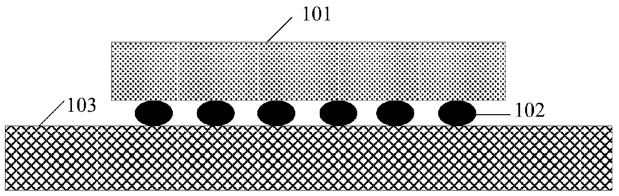
[0028] As mentioned in the background art, in the prior art, data modules are usually designed in a traditional single-sided layout and surface-mounted motherboard. The disadvantage of this type of data module is that, on the one hand, it can only adopt a single-sided layout design, and the module PCB area is large; on the other hand, it will increase the thickness of the product.

[0029] figure 1 It is a structural schematic diagram of a printed circuit board in the prior art. Such as figure 1 As shown, the current printed circuit board includes a PCB sub-board 101 , a PCB mother board 103 and a plurality of solder balls 102 . In the printed circuit board, the PCB sub-board 101 is surface-attached to the PCB mother board 103 and fixed by solder balls 102 , so the cost is relatively low. However, because this assembly method can only be laid out on one side, the area is too large, and the PCB layout area may even be doubled, and the PCB area of ​​the data module obtained b...


PUM


Abstract

The invention discloses a printed circuit board and a manufacturing method thereof and a terminal, and the printed circuit board comprises: a printed circuit board daughter board which is a radio frequency printed circuit board; a printed circuit board mother board, wherein the printed circuit board mother board is provided with a hollow groove, and the printed circuit board daughter board is embedded into the hollow groove. The radio frequency printed circuit board provided by the invention is beneficial to reducing the total thickness of equipment assembly.

Description

technical field [0001] The invention relates to the technical field of printed circuit boards, in particular to a printed circuit board, a manufacturing method thereof, and a terminal. Background technique [0002] In the prior art, various modules are usually designed in a traditional single-sided layout and surface-mounted motherboard. Specifically, most of the traditional data modules are laid out on one side, and then surface-mounted on the printed circuit board through the module Leadless Chip Carriers (LCC package) or contact array package (Land Grid Array, LGA package). Board (Printed Circuit Board, referred to as PCB) motherboard. The advantage of the surface mount method is that it is low in cost and easy to be promoted on a large scale. However, due to the large PCB area of ​​the data module, the thickness of the whole product will be increased after surface mounting, which does not meet the expectations of the thinner and thinner overall thickness of electronic c...

Claims


Application Information

Patent Timeline
Patent Type & Authority Applications(China)
IPC IPC(8): H05K1/14H05K3/36
CPCH05K1/142H05K3/36H05K2201/048H05K2201/049H05K1/141H05K2201/09845H05K2201/10098H05K1/0243H05K2203/0207H05K3/0047
Inventor 蔡元元王志钢
Owner SPREADTRUM COMM (SHANGHAI) CO LTD
Why Eureka
Try Eureka