Preparation method of avalanche photodiode diffusion structure and diode diffusion structure

An avalanche photoelectric and diffusion structure technology, applied in the field of photodetectors, can solve the problems of complexity and cost reduction, increase of breakdown voltage deviation, external circuit, high cost, etc., to reduce relative deviation, improve sample yield, The effect of improving the yield rate

Active Publication Date: 2021-04-23
UNIV OF SCI & TECH OF CHINA
View PDF5 Cites 0 Cited by
  • Summary
  • Abstract
  • Description
  • Claims
  • Application Information

AI Technical Summary

Problems solved by technology

Although the breakdown voltage deviation in the array can be compensated according to the test structure, this test and compensation device is complex and expensive, and it is not universal, and in imaging sensors, position sensors, etc., the impact of breakdown voltage changes is destructive
The breakdown voltage deviation in this array increases the complexity and cost of the external circuit and also degrades the performance of the avalanche photodiode array to some extent.

Method used


Image

  • Preparation method of avalanche photodiode diffusion structure and diode diffusion structure
  • Preparation method of avalanche photodiode diffusion structure and diode diffusion structure
  • Preparation method of avalanche photodiode diffusion structure and diode diffusion structure

Examples


preparation example Construction

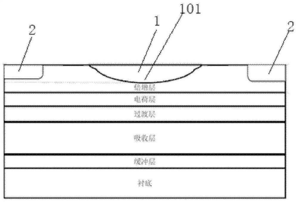
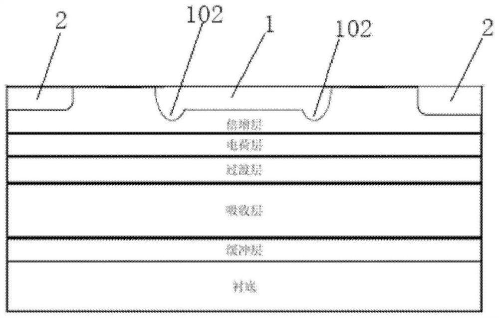
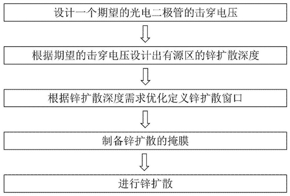
[0035] An embodiment of the present invention provides a method for preparing an avalanche photodiode diffusion structure, see figure 1 with figure 2 , the method includes: on the epitaxial wafer of the avalanche photodiode, under the effect of the first photolithography mask, perform the first dopant diffusion to obtain the central circular diffusion main junction region 1 and the diffusion main junction region 1 Diffusion tank regions 2 separated by a preset distance; under the action of the second photolithography mask, the second dopant diffusion is performed, so that the depth of the central region 101 or edge region 102 of the diffusion main junction region is greater than that of the through The depth of the diffusion main junction region is obtained by the first dopant diffusion, thereby obtaining the avalanche photodiode diffusion structure.

[0036] The embodiment of the present invention is illustrated by taking the first dopant diffusion and the second dopant dif...

Embodiment 1

[0050] In this embodiment, a 32*32 avalanche photodiode array is selected, and nearly 100 points are selected from it to test the breakdown voltage. The avalanche photodiode includes a central circular diffusion main junction region 1 , a diffusion tank region 2 , and two guard ring regions 3 between the diffusion main junction region 1 and the diffusion groove region 2 .

[0051] The test results are as Figure 10 As shown, it can be seen that the maximum breakdown voltage value in the test results does not exceed 75.1V, and the minimum value is greater than 74.3V, that is, the breakdown voltage deviation is <±0.4V, and the relative voltage deviation is <±1%.

[0052] It shows that the avalanche photodiode of this embodiment suppresses the edge breakdown and ensures a large breakdown voltage, and the uniformity of the breakdown voltage is excellent.

[0053] Another embodiment of the present invention also provides an avalanche photodiode diffusion structure, which includes:...


PUM

PropertyMeasurementUnit
diameteraaaaaaaaaa
breakdown voltageaaaaaaaaaa

Abstract

The invention provides a preparation method of an avalanche photodiode diffusion structure and a diode diffusion structure. The method includes: on the epitaxial wafer of the avalanche photodiode, under the action of the first photolithography mask, perform the first dopant diffusion to obtain the central circular diffusion main junction region (1) and the diffusion main junction region (1). Diffusion tank regions (2) with a predetermined distance between the junction regions; under the action of the second photolithography mask, a second dopant diffusion is performed, so that the central region (101) or edge region of the diffusion main junction region The depth of (102) is greater than the depth of the diffused main junction region obtained through the first dopant diffusion, thereby obtaining an avalanche photodiode diffused structure. The uniformity of chip breakdown voltage is regulated while suppressing edge breakdown.

Description

technical field [0001] The invention relates to the field of photodetectors, in particular to a preparation method of an avalanche photodiode diffusion structure and a diode diffusion structure. Background technique [0002] Avalanche photodiodes of III-V semiconductor materials are widely used in near-infrared photodetection and other related fields, such as optical fiber communication systems, near-infrared detection fields, and quantum communication single-photon detection. An avalanche photodiode (Separate Absorption and Multiplication Avalanche Photodiode: SAM-APD) structure with a separate absorption and multiplication layer can provide an electrical signal output with high fidelity (ie, low noise). On this basis, an avalanche photodiode (Separate, Absorption, Grading, Charge and Multiplication Avalanche Photodiode: SAGCM-APD) with a separate charge control layer and transition layer is added, which optimizes the electric field distribution of the device and reduces th...

Claims


Application Information

Patent Timeline
Patent Type & Authority Patents(China)
IPC IPC(8): H01L31/0352H01L31/107H01L31/18
CPCH01L31/0352H01L31/107H01L31/18
Inventor 王亮张博健秦金
Owner UNIV OF SCI & TECH OF CHINA
Why Eureka
Try Eureka