Testing device and testing method for Internet of Things semiconductor equipment

A test device, semiconductor technology, applied in the direction of measuring devices, optical devices, instruments, etc., can solve the problems of long time consumption and low detection efficiency, achieve accurate detection results and improve detection efficiency

Inactive Publication Date: 2020-04-14
王东
View PDF14 Cites 3 Cited by
  • Summary
  • Abstract
  • Description
  • Claims
  • Application Information

AI Technical Summary

Problems solved by technology

[0005] In the prior art, laser sensing technology is commonly used to detect the surface flatness of semiconductor equipment, but they all use one-by-one detection, that is, to detect the surface of a single semiconductor device one by one, which takes a long time and has low detection efficiency.

Method used


Image

  • Testing device and testing method for Internet of Things semiconductor equipment
  • Testing device and testing method for Internet of Things semiconductor equipment
  • Testing device and testing method for Internet of Things semiconductor equipment

Examples


Embodiment 1

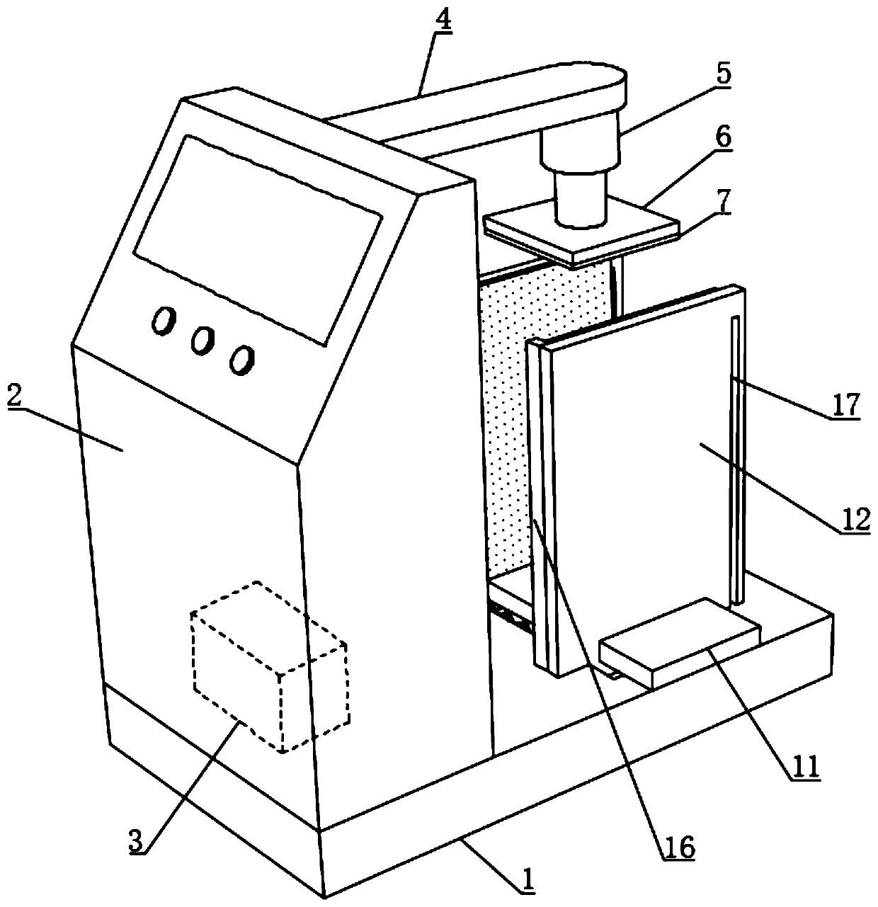
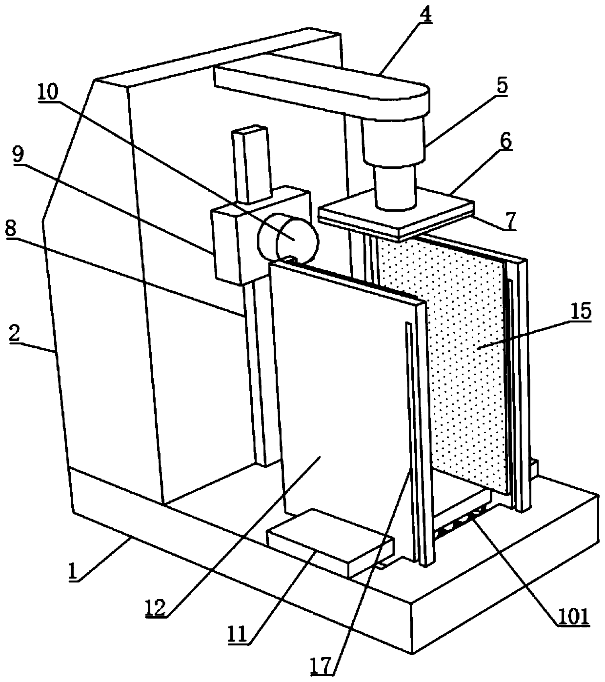
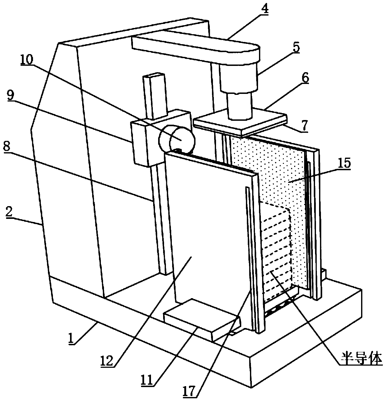
[0042] see figure 1 , a test device for semiconductor equipment of the Internet of Things, comprising a test host 2, a control panel is arranged on the test host 2, a base 1 is fixedly connected to the lower end of the test host 2, and a main control board 3 is installed inside the test host 2, The upper side of the base 1 is provided with a pair of splints 12 parallel to each other, and the splints 12 are located on one side of the test host 2. Please refer to figure 2 The upper end of the base 1 is dug with a main chute 101, the lower end of the splint 12 is slidably connected to the inside of the main chute 101, the upper end of the base 1 is fixedly connected with a backing plate 11, and the backing plate 11 is located on the upper side of the main chute 101, A rectangular hole is drilled on the splint 12, the backing plate 11 is located inside the rectangular hole, and the splint 12 is slidably connected to the outside of the backing plate 11 through the rectangular hole...


PUM


Abstract

The invention discloses a testing device and a testing method for Internet of Things semiconductor equipment. The invention belongs to the technical field of semiconductor equipment detection. The testing device comprises a testing host; a control panel is arranged on the test host; the lower end of the test host is fixedly connected with a base; a main control board is installed in the test host;a pair of parallel clamping plates is arranged on the upper side of the base; the clamping plates are positioned at one side of the test host; a main sliding groove is dug in the upper end of the base; and the lower end of eachclamping plate is slidably connected into the main sliding groove. According to the invention, a plurality of semiconductor equipments are stacked together to form a semiconductor equipment group; the semiconductor equipment group is scanned and imaged through the laser imaging technology, so that the surface flatness of multiple pieces of semiconductor equipment can bedetected at one time, multiple pieces of semiconductor equipment which do not meet the requirements can be quickly and accurately detected at one time, and the detection efficiency of the semiconductor equipment is greatly improved.

Description

technical field [0001] The invention relates to the technical field of semiconductor equipment testing, and more specifically, to a testing device and a testing method for semiconductor equipment of the Internet of Things. Background technique [0002] A semiconductor refers to a material with controllable conductivity ranging from an insulator to a conductor. The conductivity of a semiconductor at room temperature is between that of a conductor and an insulator. Semiconductors are used in integrated circuits, consumer electronics, communication systems, photovoltaic power generation, lighting applications, high-power power conversion and other fields. For example, a diode is a device made of a semiconductor. No matter from the perspective of technology or economic development, the importance of semiconductors is enormous. The core units of most of today's electronic products, such as computers, mobile phones or digital recorders, are closely related to semiconductors. Co...

Claims


Application Information

Patent Timeline
Patent Type & Authority Applications(China)
IPC IPC(8): G01B11/30
CPCG01B11/30
Inventor 王东
Owner 王东
Why Eureka
Try Eureka