Semiconductor device and forming method thereof

A semiconductor and device technology, applied in the field of semiconductor devices and their formation, can solve the problem of low semiconductor performance and achieve good performance

Inactive Publication Date: 2020-04-17
SEMICON MFG INT (SHANGHAI) CORP +1
View PDF6 Cites 0 Cited by
  • Summary
  • Abstract
  • Description
  • Claims
  • Application Information

AI Technical Summary

Problems solved by technology

[0004] However, the contact holes formed in the prior art are easy to connect with t...

Method used


Image

  • Semiconductor device and forming method thereof
  • Semiconductor device and forming method thereof
  • Semiconductor device and forming method thereof

Examples


Embodiment Construction

[0027] As mentioned in the background, the performance of the semiconductor device is poor.

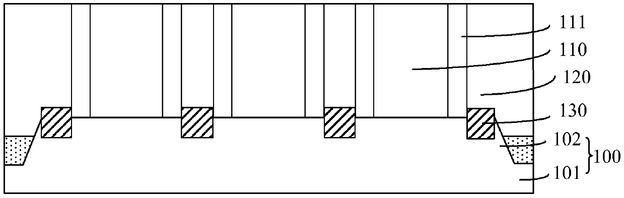
[0028] Figure 1 to Figure 4 It is a structural schematic diagram of each step of a method for forming a semiconductor device.

[0029] Please refer to figure 1 , provide a substrate 100, the substrate 100 has an initial gate structure 110 and a dielectric layer 120, the surface of the sidewall of the initial gate structure 110 has spacers 111, the substrate 100 on both sides of the initial gate structure 110 and the spacer 111 There is a source-drain doped region 130 inside, the dielectric layer 120 covers the sidewalls of the initial gate structure 110 and the spacer 111 , and the top surface of the dielectric layer 120 is flush with the top surface of the initial gate structure 110 .

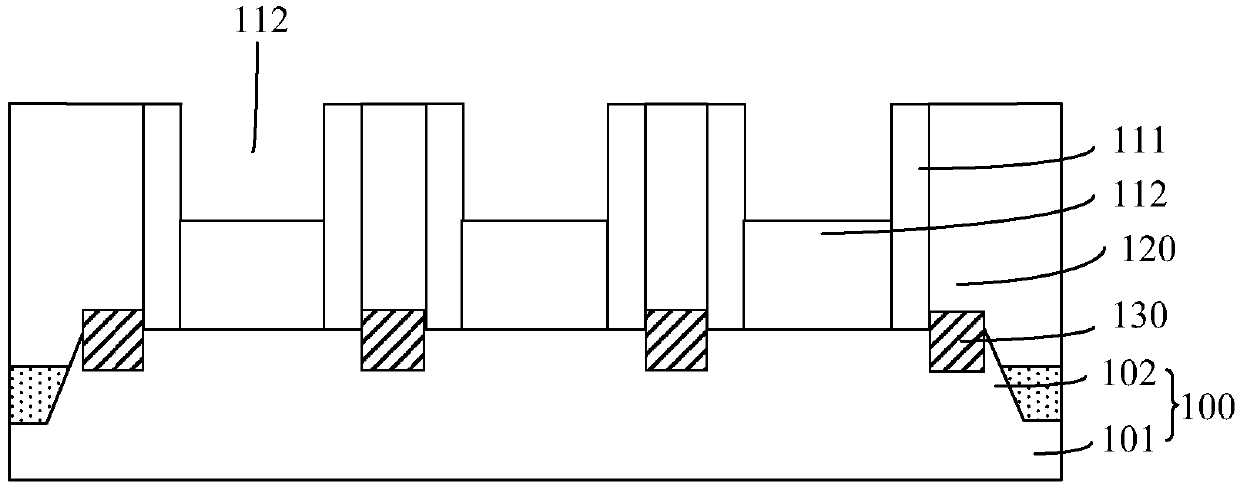
[0030] Please refer to figure 2 Part of the gate structure 110 is etched away to form a gate structure 112 , and a gate opening 112 is formed in the dielectric layer 120 .

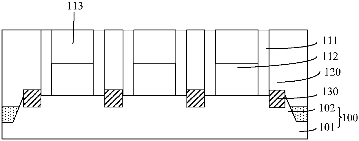
[0031] Please refer ...


PUM

PropertyMeasurementUnit
Thicknessaaaaaaaaaa

Abstract

The invention discloses a semiconductor device and a forming method thereof. The method comprises the steps of: providing a substrate, enabling the substrate to be provided with an initial gate structure, enabling the side wall surface of the initial gate structure to be provided with a side wall, enabling the initial gate structure and the substrate at two sides of the side wall to be internallyprovided with source-drain doped regions, and enabling the substrate to be provided with a dielectric layer covering the initial gate structure and the side wall, etching back a part of the initial gate structure to form a gate structure, and forming a gate opening in the dielectric layer, the top surface of the gate structure being lower than the top surface of the dielectric layer, and the sidewall of the gate opening exposing a part of the side wall, forming a protective layer in the gate opening, the protective layer covering the bottom surface and the side wall surface of the gate opening and the top surface of the dielectric layer, and the protective layer being made of a material different from that of the side wall, and after the protective layer is formed, forming an isolation structure in the gate opening, the material of the isolation structure being different from that of the protective layer. The semiconductor device formed by the method is good in performance.

Description

technical field [0001] The invention relates to the field of semiconductor manufacturing, in particular to a semiconductor device and a forming method thereof. Background technique [0002] A MOS (metal-oxide-semiconductor) transistor is an important semiconductor device. The basic structure of a MOS transistor includes: a semiconductor substrate; a gate structure located on the surface of the semiconductor substrate; a semiconductor substrate located on one side of the gate structure The source region and the drain region in the semiconductor substrate on the other side of the gate structure. [0003] With the further reduction of feature size, there are more and more process links that affect the performance and reliability of integrated circuits. At present, in the manufacturing process of semiconductor devices, contact holes (Contact, CT), as a channel connecting an active region of the device with an external circuit, play an important role in the composition of the de...

Claims


Application Information

Patent Timeline
IPC IPC(8): H01L21/8234H01L27/088
CPCH01L21/823431H01L21/823475H01L27/0886
Inventor 纪世良刘盼盼
Owner SEMICON MFG INT (SHANGHAI) CORP
Why Eureka
Try Eureka