Bare core with electromagnetic shielding structure

An electromagnetic shielding structure and bare core technology, applied in circuits, electrical components, electrical solid devices, etc., can solve the problems of high cost and complicated electromagnetic shielding structure process, and achieve the effect of low cost and simple process.

Inactive Publication Date: 2020-04-21
QIANDU TONGCHIP XIAMEN MICROELECTRONICS TECH CO LTD
View PDF4 Cites 1 Cited by
  • Summary
  • Abstract
  • Description
  • Claims
  • Application Information

AI Technical Summary

Problems solved by technology

[0003] The purpose of the present invention is to solve the problem of complex process and high cost of the electromagnetic shielding structure commonly used in integrated circuits, and provides an electromagnetic shielding structure designed at the front end of the integrated circuit. Electromagnetic shielding effect

Method used


Image

  • Bare core with electromagnetic shielding structure
  • Bare core with electromagnetic shielding structure
  • Bare core with electromagnetic shielding structure

Examples


specific Embodiment approach 1

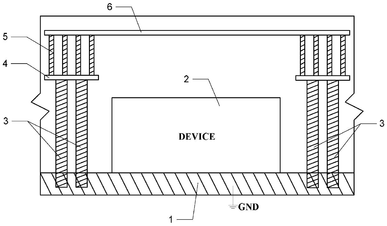
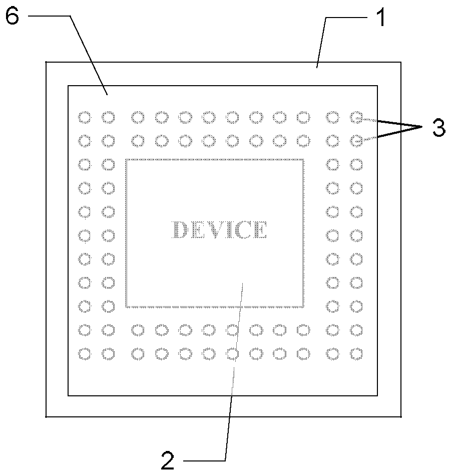
[0031] Specific implementation mode one: the following combination figure 1 , 2 and 4 illustrate this implementation mode. The bare core with an electromagnetic shielding structure described in this implementation mode is constructed using DSV technology, including a P-type substrate 1, an integrated circuit device DEVICE2, a deep silicon via DSV3, an intermediate metal layer 4, and a metal layer through The hole via5 and the top metal layer 6 are physically connected to the ground GND of the P-type substrate 1;

[0032] The integrated circuit device DEVICE2 is built on the P-type substrate 1; the multi-layer deep through-silicon via DSV3 is built tightly and orderly around the integrated circuit device DEVICE2, and the deep through-silicon via DSV3 is filled with a high-conductivity conductor, and the deep through-silicon via DSV3 The bottom end of the deep through-silicon via DSV3 penetrates the active layer of the P-type substrate 1, and the top of the deep through-silicon...

specific Embodiment approach 2

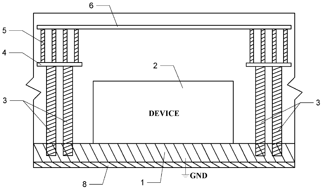
[0042] Specific implementation mode two: the following combination image 3 This embodiment will be described. The difference between this embodiment and Embodiment 1 is that the back gold 8 is bonded to the back of the P-type substrate 1 through the prepared conductive resin layer.

[0043] On the back of the P-type substrate (P++Substrate), make a layer of conductive resin and then glue the backside metal 8 (BacksideMetal). The metal material of the backside gold 8 is such as but not limited to: aluminum (Al), gold (Au ), silver (Ag), copper (Cu), adding this piece of metal can further strengthen the anti-electromagnetic ability of the structure.

specific Embodiment approach 3

[0044] Specific implementation mode three: the following combination Figure 5 Describe this embodiment mode. The difference between this embodiment mode and Embodiment 1 or 2 is that it also includes the sub-top metal layer 7, and the sub-top metal layer 7 is connected to the top metal layer 6 and the middle metal layer 4 through multiple parallel rows. The metal layer is connected via via5.

[0045] If the thickness of the top metal layer 6 cannot meet the minimum requirement of the magnetic penetration depth at the high resonant frequency, the second top metal layer 7 can also be reserved, and the interlayer oxide ILO ( To prevent short circuit between the two), the metal layer through hole via5 is constructed in the interlayer oxide layer to realize the electrical connection between the top metal layer 7 and the top metal layer 6; the deep silicon via DSV3 passes through one or more intermediate metal layers 4 It is connected to the second top metal layer 7, and other con...


PUM


Abstract

The invention discloses a bare core with an electromagnetic shielding structure, belongs to the technical field of integrated circuits, and aims to solve the problems of complex process and high costof a common electromagnetic shielding structure of an integrated circuit. The scheme of the invention is as follows: an integrated circuit device DEVICE is built on a P-type substrate; a plurality oflayers of deep silicon through holes DSV are tightly and orderly built around the integrated circuit device DEVICE, the deep silicon through holes DSV are filled with high-conductivity conductors, thebottom ends of the deep silicon through holes DSV penetrate through the active layer of the P-type substrate, and the top ends of the deep silicon through holes DSV are connected with a middle metallayer which is physically grounded; one or more middle metal layers are connected to the top metal layer, and the middle metal layers and the top metal layer are connected through multiple rows of parallel metal layer through holes via; any two middle metal layers are connected through a plurality of rows of parallel metal layer through holes via; and the top metal layer is located right above theintegrated circuit device DEVICE.

Description

technical field [0001] The invention belongs to the technical field of integrated circuits. Background technique [0002] Through multiple processes on an independent substrate, the basic device DVICE with different functions is manufactured, and these basic devices are interconnected by using multi-layer metal to form an analog integrated circuit, a digital integrated circuit or a digital-analog hybrid circuit. Some high-precision, high-sensitivity analog circuits are susceptible to interference from digital circuits, and electromagnetic waves generated by other high-frequency devices outside the chip will also damage the integrity of the output signal of the analog circuit, thereby reducing the quality of the integrated circuit and improving the quality of the integrated circuit. Design difficulty. In order to isolate the integrated circuit susceptible to electromagnetic interference from other circuits or external space, a common practice is to add a fully-enclosed metal...

Claims


Application Information

Patent Timeline
Patent Type & Authority Applications(China)
IPC IPC(8): H01L23/552
CPCH01L23/552
Inventor 李景虎周媛媛涂航辉陈日清
Owner QIANDU TONGCHIP XIAMEN MICROELECTRONICS TECH CO LTD
Why Eureka
Try Eureka