Substrate electric leakage isolation structure of conventional tunneling field effect transistor, and process method

A technology of tunneling field effect and substrate leakage, which is applied in the field of micro-nano electronics, can solve the problems of off-state current and static power consumption rise, threshold voltage drop, etc., and achieve the effect of reducing distance, suppressing leakage, and simple preparation process

Pending Publication Date: 2020-10-16
PEKING UNIV
View PDF4 Cites 0 Cited by
  • Summary
  • Abstract
  • Description
  • Claims
  • Application Information

AI Technical Summary

Problems solved by technology

From the device level, reducing the power supply voltage can effectively reduce the power consumption of the circuit. However, in order to maintain sufficient

Method used


Image

  • Substrate electric leakage isolation structure of conventional tunneling field effect transistor, and process method
  • Substrate electric leakage isolation structure of conventional tunneling field effect transistor, and process method
  • Substrate electric leakage isolation structure of conventional tunneling field effect transistor, and process method

Examples


Embodiment 1

[0074] A conventional tunneling field effect transistor substrate leakage isolation structure and process method. First, doping with boron (B) to obtain a P-type substrate. The oxide layer is deposited in an anisotropic manner, and then PWELL is injected, and boron is injected in three times. Next, the N-well is implanted, and phosphorus is implanted in an anisotropic method, and the oxide layer is etched in an anisotropic method. The next step is to make shallow trench isolation, etch the silicon in an anisotropic way, and then deposit an oxide layer in an anisotropic way. Then make the P-type doped region and the N-type doped region of the two devices. The N-type doped area is implanted with arsenic by ion implantation, and the P-type doped area is implanted with BF by ion implantation. 2 . Next, make the gate oxide layer, deposit an oxide layer on the whole piece in an anisotropic manner, and then etch away the oxide layer in the non-gate area in an anisotropic manner.

[...

Embodiment 2

[0093] In the following, the present invention will be further described through embodiments with reference to the accompanying drawings.

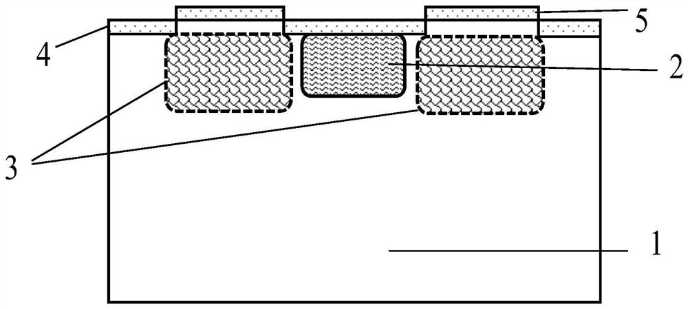
[0094] Such as figure 1 As shown, the active area is made in the NWELL, and the injected PWELL in the middle of the NWELL. When the leakage current comes out of the high-potential device, it will pass through the equivalent reverse PN junction formed by the NWELL and PWELL, and the leakage current is greatly suppressed. . As shown in Figure 2, the process steps are as follows:

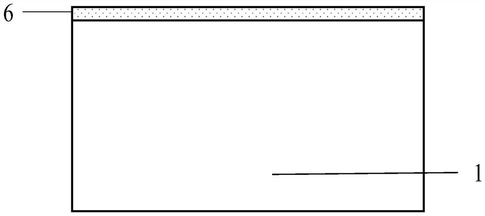
[0095] 1) Deposit an oxide layer on the P-type substrate in an anisotropic manner with a thickness of 0.012 μm, as shown in Figure 2 (a).

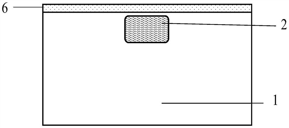
[0096] 2) Inject dose = 1.7e13cm in the PW injection area -2 , Energy=160keV and dose=9.5e12cm -2 , Energy=240keV and dose=7.9e12cm -2 , Energy=27keV boron to form PWELL. As shown in Figure 2 (b).

[0097] 3) Inject dose=2e13cm- in the NW injection zone 2 , Energy = 330kev of phosphorus. As shown in Figure 2 (c)

[0098] 4) The oxid...

Embodiment 3

[0103] A conventional tunneling field effect transistor substrate leakage isolation structure, including a P-type substrate, an active area on the P substrate, and shallow trench isolation outside the active area, the active area is surrounded by NWELL; two adjacent ones Between NWELL is PWELL. One NWELL is made of P-type TFET, and the other NWELL is made of N-type TFET.

[0104] P-type substrate doping concentration is 2e15cm- 3 .

[0105] The injection dose of NWELL is 1e13cm -2 , The energy is 340kev.

[0106] PWELL is injected in three times, and the injection dose and energy are dose = 1.5e13cm -2 , Energy=150keV; dose=9e12cm -2 , Energy=230kev; dose=7.8e12cm -2 , Energy=25keV.

[0107] Source and drain doped regions of TFET, P-type doping adopts BF 2 , The dose is 4e15cm -2 , The energy is 3kev; N-type doping uses arsenic, the dose is 1e15cm -2 , The energy is 5kev;

[0108] A conventional tunneling field effect transistor substrate leakage isolation structure process method inc...


PUM

PropertyMeasurementUnit
Thicknessaaaaaaaaaa
Thicknessaaaaaaaaaa
Thicknessaaaaaaaaaa

Abstract

The invention provides a substrate electric leakage isolation structure of a conventional tunneling field effect transistor, and a process method, and belongs to the technical field of micro-nano electronics. The structure comprises a P-type substrate, wherein an active region is arranged on the P-type substrate, shallow groove isolation is arranged outside the active region, the active region issurrounded by NWELLs, a PWELL is arranged between every two adjacent NWELLs, and the width of the PWELL between every two adjacent NWELLs is equal to or slightly smaller than the distance between every two NWELLs. According to the invention, after PWELL injection is introduced, the reverse PN junction realized by the PWELL with small width and the NWELL has a good electric leakage isolation effect, so that by using the structure provided by the invention, the electric leakage of the substrate can be effectively isolated, the distance between the TFET devices during integration can be reduced,and the optimization of the circuit area is brought.

Description

Technical field [0001] The invention relates to a substrate leakage isolation structure and a process method of a conventional tunneling field effect transistor, belonging to the technical field of micro-nanoelectronics, and specifically relates to a substrate leakage isolation of a conventional tunneling field effect transistor. Background technique [0002] With the continuous advancement of semiconductor technology, device sizes continue to decrease, circuit performance continues to improve, and chip power density increases sharply. Low power consumption has become an important design direction. From the device level, reducing the power supply voltage can effectively reduce the power consumption of the circuit. However, in order to maintain sufficient drive capability, the threshold voltage of the MOSFET device must also be lowered, resulting in an increase in off-state current and static power consumption. Conventional tunneling field effect transistors (TFETs) use a band-ban...

Claims


Application Information

Patent Timeline
IPC IPC(8): H01L29/06H01L21/331H01L29/739
CPCH01L29/0646H01L29/66356H01L29/7391
Inventor 黄芊芊仲原陈诚郭令仪叶乐黄如
Owner PEKING UNIV
Why Eureka
Try Eureka