Reinforced transistor structure with high electron mobility and fabrication method thereof

A technology of high electron mobility and manufacturing method, which is applied in the field of modulation and doping enhanced high electron mobility transistor structure and its manufacture, can solve the problems of complex depletion-type HEMT process and high power consumption, and achieve simple process, Reduced energy consumption, the effect of low energy consumption

Inactive Publication Date: 2011-06-01
INST OF SEMICONDUCTORS - CHINESE ACAD OF SCI
View PDF0 Cites 0 Cited by
  • Summary
  • Abstract
  • Description
  • Claims
  • Application Information

AI Technical Summary

Problems solved by technology

From the perspective of easy implementation of the design, depletion-type HEMT is mainly used now, but the depletion-type HEMT process is relatively complicated and consumes a lot of power

Method used


Image

  • Reinforced transistor structure with high electron mobility and fabrication method thereof
  • Reinforced transistor structure with high electron mobility and fabrication method thereof
  • Reinforced transistor structure with high electron mobility and fabrication method thereof

Examples


Embodiment Construction

[0050] In order to make the object, technical solution and advantages of the present invention clearer, the present invention will be described in further detail below in conjunction with specific embodiments and with reference to the accompanying drawings.

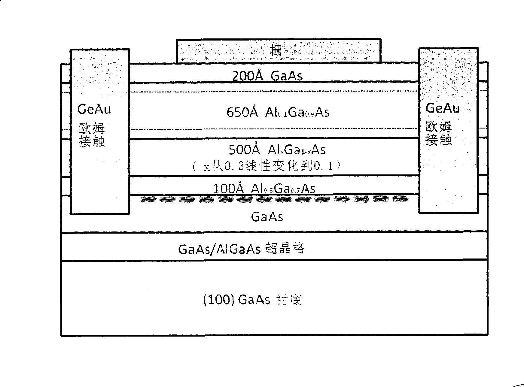
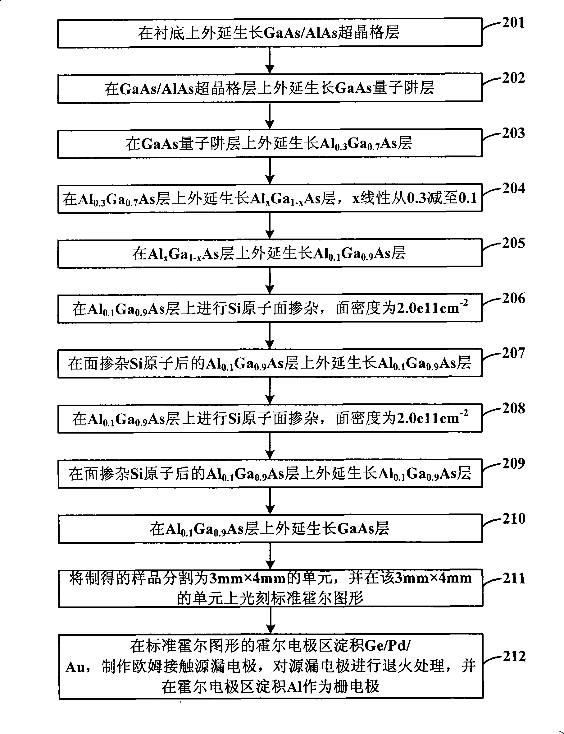
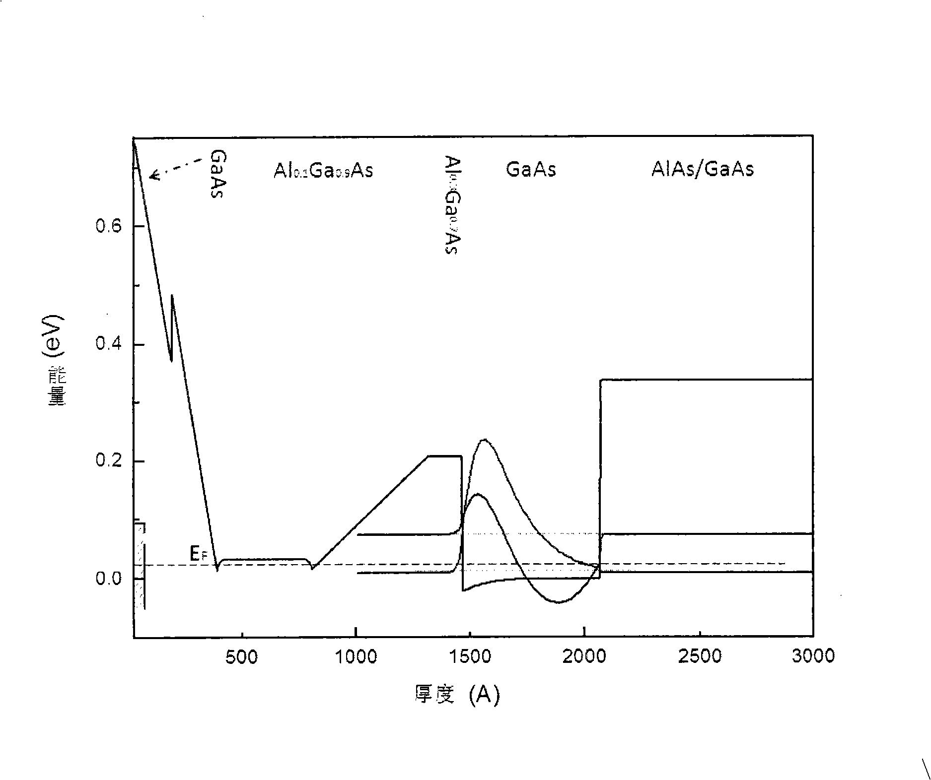
[0051] like figure 1 as shown, figure 1 It is a schematic diagram of a modulated doping-enhanced HEMT structure provided by the present invention. The structure includes from bottom to top: a semi-insulating gallium arsenide substrate with a (110) plane, and 20 cycles of GaAs / AlAs epitaxially grown on the substrate. The superlattice layer (the thickness of GaAs is 10nm, the thickness of AlAs is 10nm), the GaAs quantum well layer with a thickness of 60nm epitaxially grown on the GaAs / AlAs superlattice layer, the thickness of epitaxially grown on the GaAs quantum well layer is 10nm Al 0.3 Ga 0.7 As layer, in Al 0.3 Ga 0.7 Al with a thickness of 5nm epitaxially grown on the As layer x Ga 1-x As layer (x linearly reduc...


PUM


Abstract

The invention relates to the technical field of semiconductor devices, in particular to a modulation-doped reinforced transistor structure with high electron mobility. The reinforced transistor structure consists of a substrate, a GaAs / AlAs superlattice layer, a GaAs quantum well layer, an Al0.3Ga0.7As layer, an AlxGa1-xAs layer (x is linearly reduced from 0.3 to 0.1), an Al0.1Ga0.9As layer, a GaAs layer, source and drain electrodes and a gate electrode sequentially from the bottom up. The invention also discloses a fabrication method for the reinforced transistor structure. By utilizing the invention, the power consumption of an HEMT device is reduced, the fabrication technique is simplified, and the fabrication cost is reduced.

Description

technical field [0001] The invention relates to the technical field of semiconductor devices, in particular to a modulated doping enhanced high electron mobility transistor (HEMT) structure and a manufacturing method thereof. Background technique [0002] Over the past few decades, the rapid development of the semiconductor industry has had an incalculable impact on our society. At present, the semiconductor industry dominated by silicon and the electronics industry centered on it are the largest industries in the world. In recent years, compound semiconductors represented by gallium arsenide have attracted a lot of scientific and technological work to study the industrialization technology of the gallium arsenide-based semiconductor industry due to their attractive properties such as high-efficiency transport properties and low power consumption brought by heterostructures. Realize the feasibility of industrialization including production efficiency, yield, integrability, c...

Claims


Application Information

Patent Timeline
Patent Type & Authority Patents(China)
IPC IPC(8): H01L29/778H01L29/06H01L21/335
Inventor 谈笑天郑厚植
Owner INST OF SEMICONDUCTORS - CHINESE ACAD OF SCI
Why Eureka
Try Eureka