
Multi-channel in-situ detection device and detection method for subsurface defects of optical components

A sub-surface defect and optical element technology, applied in the field of optical elements, can solve the problems that the measurement results are greatly affected by scattering, it is difficult to accurately locate and reset the same micro-nano defect, and the detection sensitivity is low, so as to achieve compact structure and avoid influence , detect the effect of strong versatility

Active Publication Date: 2022-03-08
LASER FUSION RES CENT CHINA ACAD OF ENG PHYSICS +1
View PDF11 Cites 0 Cited by
  • Summary
  • Abstract
  • Description
  • Claims
  • Application Information

AI Technical Summary

Problems solved by technology

However, defect-induced laser damage is a very complex physical process, which is closely related to the geometric shape of the defect, photoluminescence, and photothermal absorption characteristics. Previously, a single technical method could not provide sufficient physical image information of defects, and the detection sensitivity was low. The result is highly affected by scattering
Moreover, when several methods are used for independent measurement at the same time, the influence of changes in the measurement environment cannot be avoided, and it is difficult to accurately locate and reset the same micro-nano defect

Method used


Image

  • Multi-channel in-situ detection device and detection method for subsurface defects of optical components

Examples


Embodiment

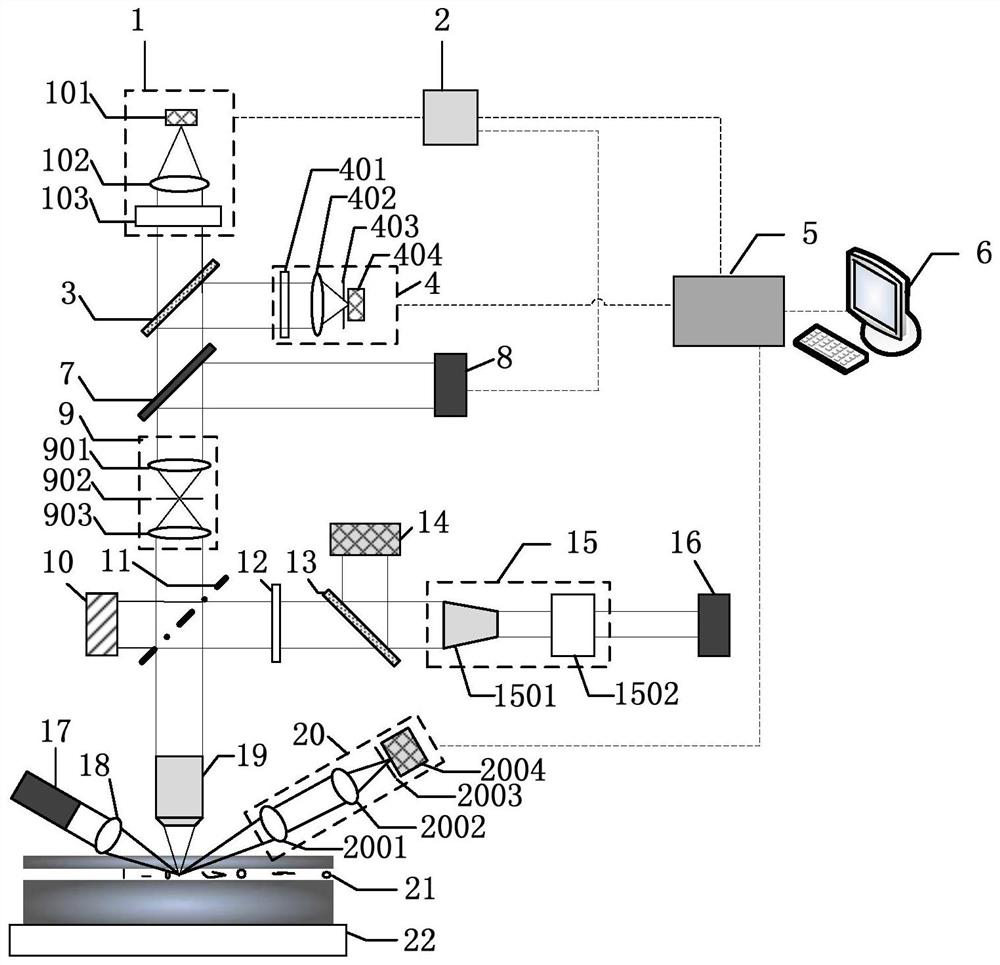
[0067] The short pulse laser light source 8 provides a picosecond high-frequency laser pulse, a wavelength of 375 nm, is used to excite optical element defects to generate photorefluorescence, and use it as an excitation signal access time-dependent single optical sub-count module 2; The dichroic mirror 7 is a long-in-chi-chromatic frame, which is high than the laser light having a wavelength of less than 375 nm, which is higher than the laser light of 375 nm, and the wavelength of the laser light source and the fluorescence wavelength is separated.

[0068] The confocal module 9 includes a lens 901, aperture 902, a lens 902, which is a co-focused detecting system 4, a microscopic amplification system 19, and the optical element 21 sub-surface constitutes a confocal system for achieving sub-surface defective Geometric high-resolution measurement, the small hole 902 diameter is 10 μm, the transverse resolution of the confocal detection system xy The wavelength of the excitation las...


PUM

PropertyMeasurementUnit
wavelengthaaaaaaaaaa
diameteraaaaaaaaaa

Abstract

A multi-channel in-situ detection device and detection method for subsurface defects of optical elements, which are used for defect testing of optical elements such as glass. The device consists of three channels: a fluorescence confocal imaging system, a fluorescence lifetime imaging system, and a photothermal absorption imaging system. test. The invention has the characteristics of compact device structure, strong detection versatility and high stability, and is suitable for high-sensitivity non-destructive detection of subsurface defects.

Description

Technical field [0001] The present invention relates to an optical element, particularly a multi-channel in-situ detecting device and a detection method of an optical element sub-surface defect. Background technique [0002] During the processing of optical components, it is inevitably to produce different degrees of defects in the sub-surface. The introduction of defects reduces the band gap width of the material, producing sub-band gap absorption (multi-photonic absorption) under strong laser mode, and the number of free electrons in the common action of multi-photonic ionization and avalanche ion increases sharply, and the collision lattice generates heat. When the energy deposition level exceeds the thermodynamic tolerance limit of the material, damage is caused, resulting in low performance of optical components or even fail. Therefore, the detection technique of conducting optical components sub-surface defects has a very important significance for improving laser damage in...

Claims


Application Information

Patent Timeline
Patent Type & Authority Patents(China)
IPC IPC(8): G01N21/88G01N21/64G01N25/20
CPCG01N21/8806G01N21/64G01N25/20
Inventor 张霖许乔石振东陈坚马骅马可白金玺李杰柴立群赵建华黄明
Owner LASER FUSION RES CENT CHINA ACAD OF ENG PHYSICS
Learn More