Power semiconductor device cell structure, preparation method thereof and power semiconductor device

A technology for power semiconductors and devices, which is applied in semiconductor/solid-state device manufacturing, electrical components, circuits, etc.

Active Publication Date: 2020-05-05
GREE ELECTRIC APPLIANCES INC +1
View PDF7 Cites 2 Cited by
  • Summary
  • Abstract
  • Description
  • Claims
  • Application Information

AI Technical Summary

Problems solved by technology

However, this approach will have a greater impact on the distribution of...

Method used


Image

  • Power semiconductor device cell structure, preparation method thereof and power semiconductor device
  • Power semiconductor device cell structure, preparation method thereof and power semiconductor device
  • Power semiconductor device cell structure, preparation method thereof and power semiconductor device

Examples


Embodiment 1

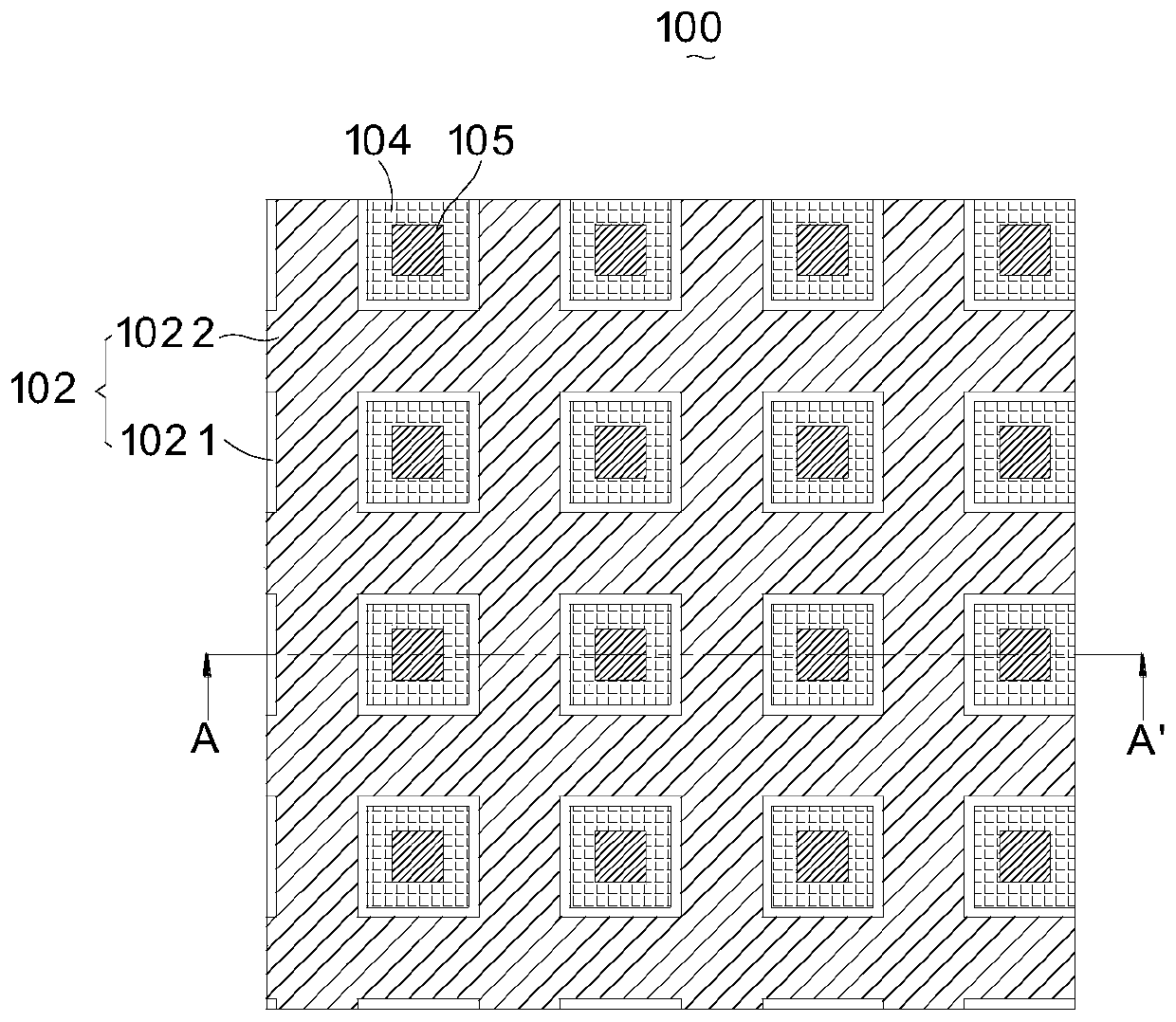
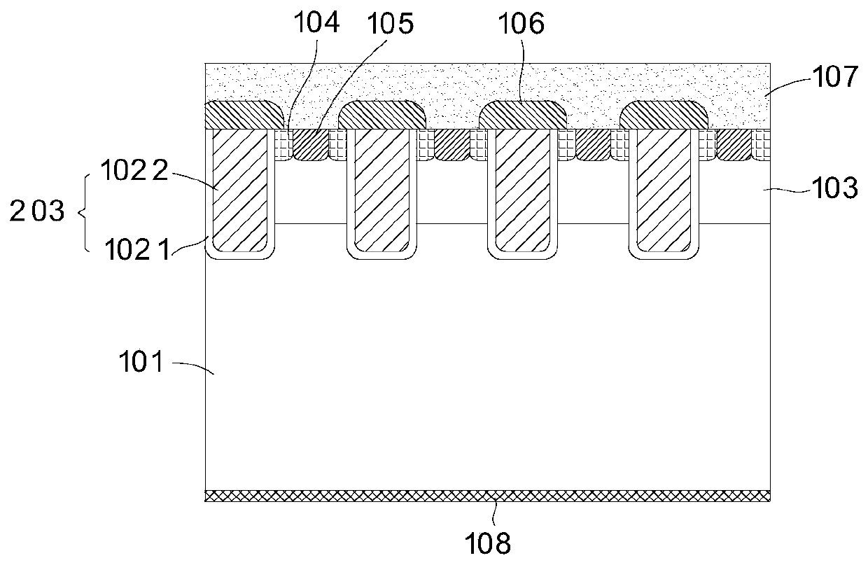
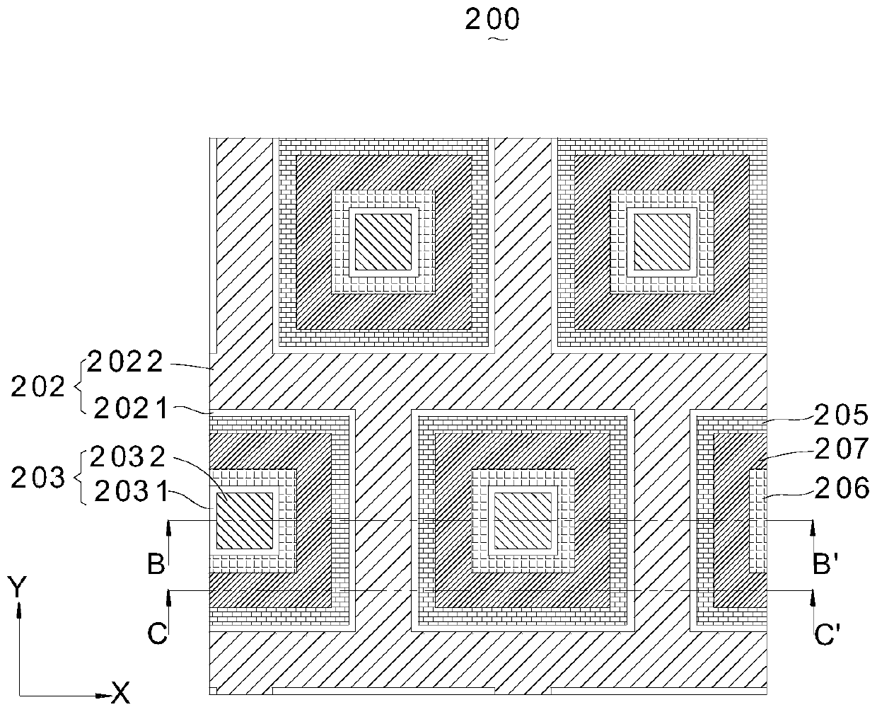
[0054] Such as Figure 3 to Figure 6 As shown, the embodiment of the present disclosure provides a power semiconductor device cell structure 200, including a substrate 201, a first trench gate 202, a second trench gate 203, a well region 204, a first source region 205, a second source region Region 206 , third source region 207 , first interlayer dielectric layer 208 , second interlayer dielectric layer 209 , emitter metal layer 210 and collector metal layer 211 .

[0055] It should be noted that, in order to image 3 with Image 6 The shapes and positions of the first trench gate 202, the second trench gate 203, the well region 204, the first source region 205, the second source region 206 and the third source region 207 are clearly shown in the figure, image 3 with Image 6 The substrate 201 , the first interlayer dielectric layer 208 , the second interlayer dielectric layer 209 , the emitter metal layer 210 and the collector metal layer 211 are not shown. but combine ...

Embodiment 2

[0075] On the basis of the first embodiment, this embodiment provides a method for preparing the cell structure 200 of a power semiconductor device. Image 6 It is a schematic flowchart of a method for preparing a power semiconductor device cell structure 200 shown in an embodiment of the present disclosure. Figure 7-Figure 12 It is a schematic cross-sectional structure formed by the relevant steps of a method for preparing a cell structure 200 of a power semiconductor device shown in an embodiment of the present disclosure. Below, refer to Figure 7 with Figure 8-Figure 13 The detailed steps of an exemplary method of the method for manufacturing the power semiconductor device cellular structure 200 proposed by the embodiment of the present disclosure will be described.

[0076] Such as Figure 7 As shown, the preparation method of the power semiconductor device cellular structure 200 in this embodiment includes the following steps:

[0077] Step S101 : providing a first...


PUM


Abstract

The invention provides a power semiconductor device and a preparation method thereof. The power semiconductor device comprises a first conductive type substrate, first trench gates arranged in the substrate and distributed in a grid shape, island-shaped second trench gate which is positioned in each grid cell enclosed by the first trench gate, a second conduction type well region which is locatedin the substrate and located between the first trench gate and the second trench gate, a first conduction type first source region, a first conduction type second source region and a second conductiontype third source region, wherein the first conduction type first source region, the first conduction type second source region and the second conduction type third source region are located in the well region. The device further comprises an emitting electrode metal layer which is positioned above the substrate and is electrically connected with the first source region, the second source region,the third source region and the second trench gate at the same time. Under the condition that the distribution of electric field lines in the device is not changed, the current density is reduced byincreasing the distance between the effective trench gates. The anti-short-circuit capability of the device is improved. The electric field in the device can be improved, and the voltage endurance capability of the device is improved.

Description

technical field [0001] The present disclosure relates to the technical field of semiconductor devices, in particular to a cell structure of a power semiconductor device, a preparation method thereof, and a power semiconductor device. Background technique [0002] Power semiconductor devices, also known as power electronic devices, include power diodes, thyristors, insulated gate bipolar transistors (IGBTs), high-power power transistors (GTRs), gate turn-off thyristors (GTOs), and metal-oxide semiconductor field-effect transistors. (MOSFETs). Power semiconductor devices are widely used in various power control circuits, drive circuits and other circuits, especially in various variable frequency motors, photovoltaic inverters and smart grids, new energy vehicles, electric locomotive traction drives and other fields. [0003] Power semiconductor devices generally consist of a cell structure, a terminal withstand voltage structure, and a transition region structure. [0004] T...

Claims


Application Information

Patent Timeline
IPC IPC(8): H01L21/67
CPCH01L21/67
Inventor 曾丹史波肖婷马颖江敖利波
Owner GREE ELECTRIC APPLIANCES INC
Why Eureka
Try Eureka