Process method of SGT device

A process method and device technology, applied in the field of semiconductor device manufacturing, can solve problems such as large gate-source leakage, and achieve the effects of uniform thickness, increased thickness, and smooth transition

Active Publication Date: 2020-05-08
SHANGHAI HUAHONG GRACE SEMICON MFG CORP
View PDF3 Cites 4 Cited by
  • Summary
  • Abstract
  • Description
  • Claims
  • Application Information

AI Technical Summary

Problems solved by technology

SGT devices whose operating voltage is above 60V have a thick pad oxide layer, and after removing the pad oxide layer, both sides of the thermal oxide layer are depressed, such as Figure 2-4 As shown, it also causes the oxide layer here to be thinner, causing the leakage between the gate and the source to be too large

Method used


Image

  • Process method of SGT device
  • Process method of SGT device
  • Process method of SGT device

Examples


Embodiment Construction

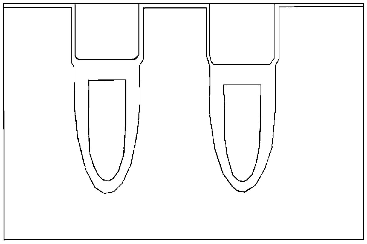
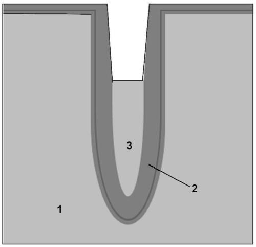
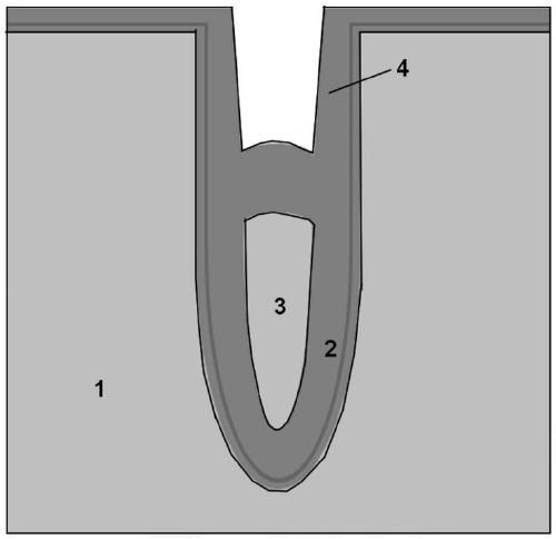
[0024] The process method of the SGT device according to the present invention is mainly aimed at forming a polysilicon source electrode and a polysilicon gate in the trench, and optimizing the morphology of its section, including the following process steps:

[0025] The first step is to form a trench gate on a heavily doped semiconductor substrate (or epitaxial). The trench gate is to form a trench on the substrate, and then deposit a dielectric layer ( The dielectric layer is a layer of silicon oxide layer close to the substrate or epitaxy on the inner wall of the trench, no reference numerals are used) and a layer of pad oxide layer, and then polysilicon is deposited and etched back to form source polysilicon, or shielding electrode polysilicon . Such as figure 2 As shown, the dielectric layer is a gate dielectric layer, such as a silicon oxide layer, and the oxide layer is attached to the inner wall of the trench as an isolation dielectric layer between the polysilicon ...


PUM

PropertyMeasurementUnit
thicknessaaaaaaaaaa
thicknessaaaaaaaaaa

Abstract

The invention discloses a process method of an SGT device. The method comprises the process steps of: 1, forming a trench type gate on a heavily doped semiconductor substrate, namely, forming a trenchon the substrate, then depositing a dielectric layer and a liner oxide layer, and then depositing polycrystalline silicon and etching back to form source polycrystalline silicon; 2, forming a thermaloxidation layer again; 3, depositing an oxide layer again by adopting an HDPCVD method; 4, removing the liner oxide layer at the upper part of the trench; and 5, depositing polycrystalline silicon and performing back etching to complete the manufacturing of the polycrystalline silicon gate at the upper part of the trench. According to the method, an HDPCVD process is added after the conventionalthermal oxide layer deposition process, so that the upper surface of the thermal oxide layer is flatter, the transition of a corner region of the trench is smoother, the defects of recesses on two sides, sharp corners and the like are avoided, and the situation of electric leakage between the polycrystalline silicon gate and a shielding electrode is not easily caused.

Description

technical field [0001] The invention relates to the field of semiconductor device manufacturing, in particular to a process method of an SGT device. Background technique [0002] In the field of medium and low voltage devices with a withstand voltage above 60V, Shield Gate Trench (SGT) devices are widely used because of their low specific on-resistance and low gate-drain coupling capacitance. The gate structure of SGT devices includes shielded polysilicon and polysilicon gate. Shielded polysilicon is usually also called source polysilicon, which are all formed in the trench. According to the different settings of shielded polysilicon and polysilicon gate in the trench, it is usually divided into upper and lower structures and left and right structures. . In the upper and lower structure, the shielding polysilicon is located at the bottom of the trench, the polysilicon gate is located at the top of the trench, and the polysilicon gate and the shielding polysilicon are in a v...

Claims


Application Information

Patent Timeline
Patent Type & Authority Applications(China)
IPC IPC(8): H01L21/28
CPCH01L29/401H01L21/28Y02T10/12
Inventor 张辉陈正嵘
Owner SHANGHAI HUAHONG GRACE SEMICON MFG CORP
Why Eureka
Try Eureka