Unlock instant, AI-driven research and patent intelligence for your innovation.

Power module packaging structure and packaging method thereof

A packaging structure and power module technology, applied in electrical components, electrical solid devices, circuits, etc., can solve the problem of small space for reducing inductance, and achieve the effects of reducing overshoot voltage, reducing switching oscillation, and improving power density

Active Publication Date: 2020-05-08
湖南国芯半导体科技有限公司
View PDF3 Cites 0 Cited by
  • Summary
  • Abstract
  • Description
  • Claims
  • Application Information

AI Technical Summary

Problems solved by technology

[0003] Wide bandgap semiconductor devices, the switching speed is faster, the problem caused by stray inductance will be more serious, the power module with traditional bonding wire structure, the space for reducing inductance is relatively small, so it is necessary to provide a power module that can significantly reduce stray Inductor power module package structure and process method

Method used


Image

  • Power module packaging structure and packaging method thereof
  • Power module packaging structure and packaging method thereof
  • Power module packaging structure and packaging method thereof

Examples


Embodiment Construction

[0044] The present invention will be further described below in conjunction with accompanying drawing.

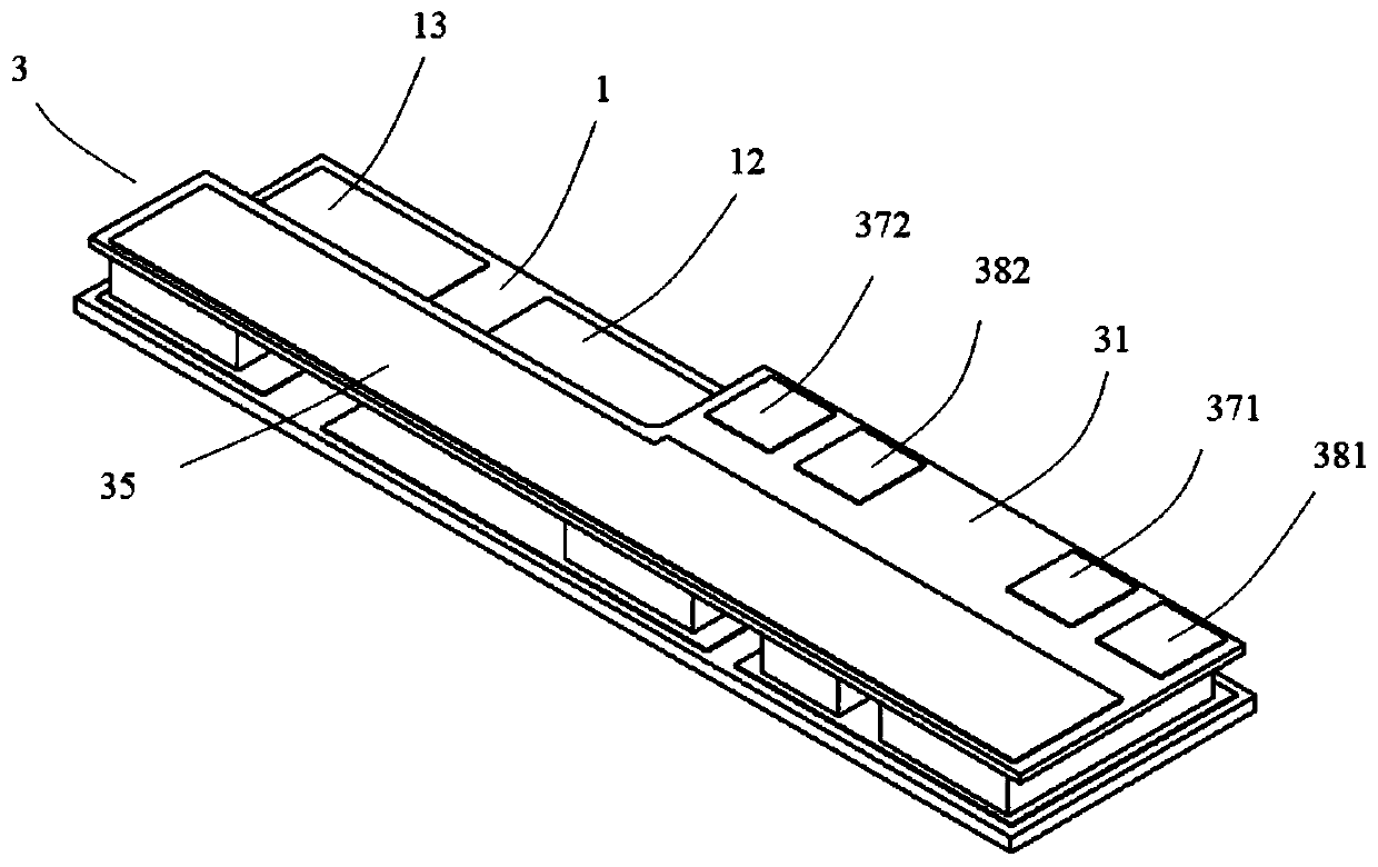
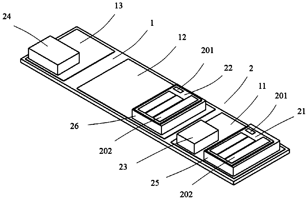
[0045] as attached figure 1 As shown, the power module packaging structure provided by the present invention includes a backing board 1, on which a module functional unit is arranged, and the upper surface of the module function unit is covered with a circuit board 3, and the circuit board 3 is used for bonding the backing board 1 and the module. functional unit.

[0046] Specifically, the circuit board 3 replaces the traditional bonding wires, together with the backing board 1 and the module functional unit, constitutes a current transmission loop for main current and control signals. as attached figure 1 As shown, the structure of the entire power module without bonding wires eliminates the need to reserve the position of bonding wires on the metal layer in the module, and does not need to consider the size of the bonding wires and whether it is convenient for the bondi...


PUM


Abstract

The invention provides a power module packaging structure and a packaging method thereof. The packaging structure comprises a lining plate, and a module function unit is arranged on the lining plate,wherein the upper surface of the module function unit is covered with a circuit board, and the circuit board is used for forming a complete current loop together with the lining plate and the module function unit. According to the packaging structure, a traditional bonding wire is replaced by the circuit board, so stray inductance of a loop is reduced; meanwhile, a laminated circuit structure is formed by the circuit board, the module function unit and the lining plate, so the stray inductance of the power module can be further reduced. According to the packaging method provided by the invention, only the circuit board, the lining plate, the module function unit and other components need to be connected, and the mutual connection positions of all the components are fixed, so rapid assemblyof the power module can be carried out; meanwhile, point contact connection of bonding wires is replaced by surface-to-surface contact connection, so better temperature distribution is achieved, andthe reliability of the power module is higher.

Description

technical field [0001] The invention relates to the technical field of semiconductor power module devices, in particular to a power module packaging structure and a packaging method thereof. Background technique [0002] A large number of bonding wires are required for the interconnection of chips and substrates in traditional power modules, and the bonding wire structure will generate certain parasitic inductance. During the turn-on and turn-off process of the power module, the current changes sharply, resulting in a large current change rate di / dt. The combined effect of parasitic inductance and current change rate di / dt will generate inductor voltage Vo, the relationship between the two is: Vo=Ls*di / dt, where Ls represents the stray inductance of the switch loop, and the parasitic voltage generated by the bonding wire Inductance is an important part of stray inductance. The superposition of the inductor voltage Vo and the bus voltage will generate a voltage spike. On th...

Claims


Application Information

Patent Timeline
IPC IPC(8): H01L23/498H01L23/367H01L25/18H01L21/60
CPCH01L23/3677H01L23/49816H01L23/49844H01L24/81H01L25/18H01L25/50H01L2224/81194
Inventor 齐放王彦刚姚亮柯攀戴小平
Owner 湖南国芯半导体科技有限公司
Features
  • R&D
  • Intellectual Property
  • Life Sciences
  • Materials
  • Tech Scout
  • Unparalleled Data Quality
  • Higher Quality Content
  • 60% Fewer Hallucinations
Learn More