Biconcave metal semiconductor resonant cavity for nano laser

A metal semiconductor and nano-laser technology, applied in the structure of optical resonators, lasers, laser parts, etc., can solve the problems of large radiation loss, large metal loss, mode dispersion, etc., to reduce radiation loss, easy to manufacture, reduce Effect of Threshold Current

Inactive Publication Date: 2020-05-08
NANJING UNIV OF SCI & TECH
View PDF2 Cites 2 Cited by
  • Summary
  • Abstract
  • Description
  • Claims
  • Application Information

AI Technical Summary

Problems solved by technology

However, the side wall of the capsule resonator is still a straight wall structure, especially the side wall near the curved end face still has a large metal loss
In addition,...

Method used


Image

  • Biconcave metal semiconductor resonant cavity for nano laser
  • Biconcave metal semiconductor resonant cavity for nano laser
  • Biconcave metal semiconductor resonant cavity for nano laser

Examples


Embodiment 1

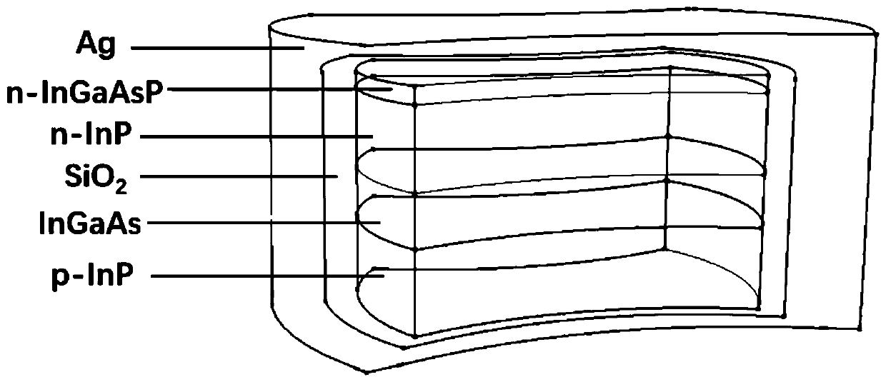
[0030] figure 1 It is a three-dimensional schematic diagram of a double-concave metal-semiconductor resonator for nano-lasers in this embodiment. The curved sidewall shape of the sidewall of the metal-semiconductor resonator is suitable for any concave curve. The cubic function resonator in this embodiment has a curved sidewall. The curve is:

[0031] y=a x 3 +W 0 / 2

[0032] Among them, y represents the width of the side wall curve in the y direction, which changes with the coordinate x, a represents the degree of curvature of the side wall curve in the concave curve, W 0 Indicates the beam waist width of the concave curve of the resonator.

[0033] Taking the cubic function curve as an example, the given function constitutes a double-concave side wall concave curve, the cavity length of the resonant cavity is L=700nm, the maximum width of the resonant cavity is W=520nm, and the beam waist width of the concave curve of the resonant cavity is W 0 =0.8W, L / R=1.43. The sem...


PUM

PropertyMeasurementUnit
Cavity lengthaaaaaaaaaa
Maximum widthaaaaaaaaaa
Thicknessaaaaaaaaaa

Abstract

The invention discloses a biconcave metal semiconductor resonant cavity for a nano laser. The biconcave metal semiconductor resonant cavity comprises a semiconductor layer, an insulating layer and a metal layer which are sequentially arranged from inside to outside, wherein the semiconductor layer comprises an InGaAs core layer, a p-doped InP material layer, an n-doped InP material layer and a p-doped InGaAs top contact layer; the lower layer of the InGaAs core layer is a p-doped InP material layer, the upper layer of the InGaAs core layer is an n-doped InP material layer, and a p-doped InGaAstop contact layer is arranged on the n-doped InP material layer; the insulating layer is made of an insulator material SiO<2>, and wraps the side wall and the end surface of the semiconductor layer;and the metal layer is made of a metal material Ag, wraps the insulating layer and is in contact with the semiconductor layer at the top. According to the invention, the radiation loss is reduced, themetal surface plasmon loss is reduced, the structure is simple, the manufacturing is easy, and the threshold current for exciting the resonant cavity is effectively reduced.

Description

technical field [0001] The invention belongs to the technical field of semiconductor nano-lasers, in particular to a double-concave metal-semiconductor resonator used in nano-lasers. Background technique [0002] As an ultra-small light source, metal-semiconductor nanolasers have been widely studied, and they have a wide range of applications in photonic integrated circuits, on-chip optical interconnects, and optical communications. As the volume of the resonator decreases, the loss of the laser increases rapidly, which hinders the further miniaturization of the laser. Currently popular metal-semiconductor nanolasers include two modes, one is the whispering-galley mode and the other is the Fabry-Perot mode. The former has a higher quality factor, but is not conducive to waveguide coupling. The latter typically have a lower quality factor due to the reflection loss of the resonator, but have the advantage of easy coupling of mode energy into the integrated waveguide. [000...

Claims


Application Information

Patent Timeline
IPC IPC(8): H01S5/10H01S5/30H01S5/323
CPCH01S5/1057H01S5/3009H01S5/3013H01S5/323
Inventor 张柏富朱康武恒胡海峰
Owner NANJING UNIV OF SCI & TECH
Why Eureka
Try Eureka