
Multi-wake-up-source input low-power-consumption chip architecture system and quick starting method

A technology of low power consumption and wake-up source, which is applied in the direction of instruments, electrical digital data processing, digital data processing components, etc., can solve the problems of high power consumption, speed-up chips, and slow startup of smart lock chips, so as to reduce power consumption, The effect of reducing power consumption and reducing sleep power consumption

Pending Publication Date: 2020-05-12
ANYKA (GUANGZHOU) MICROELECTRONICS TECH CO LTD
View PDF6 Cites 6 Cited by
  • Summary
  • Abstract
  • Description
  • Claims
  • Application Information

AI Technical Summary

Problems solved by technology

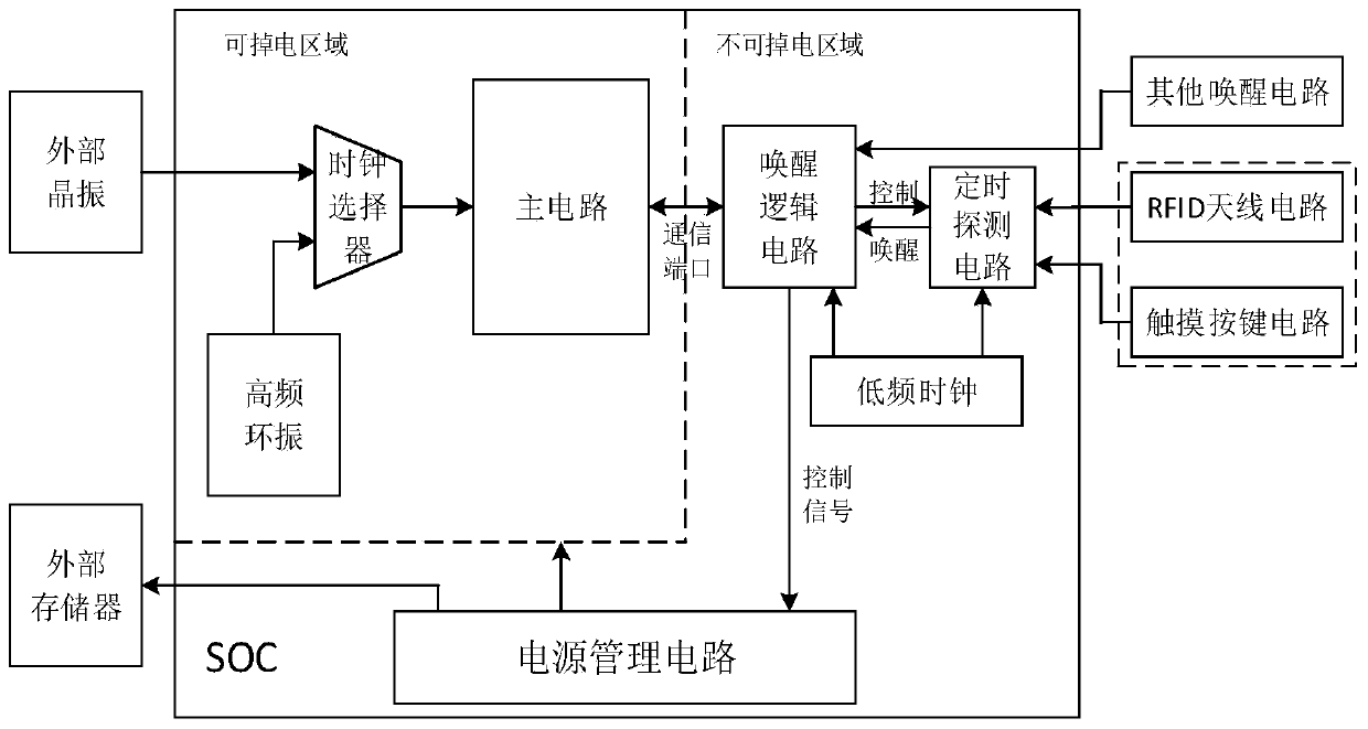
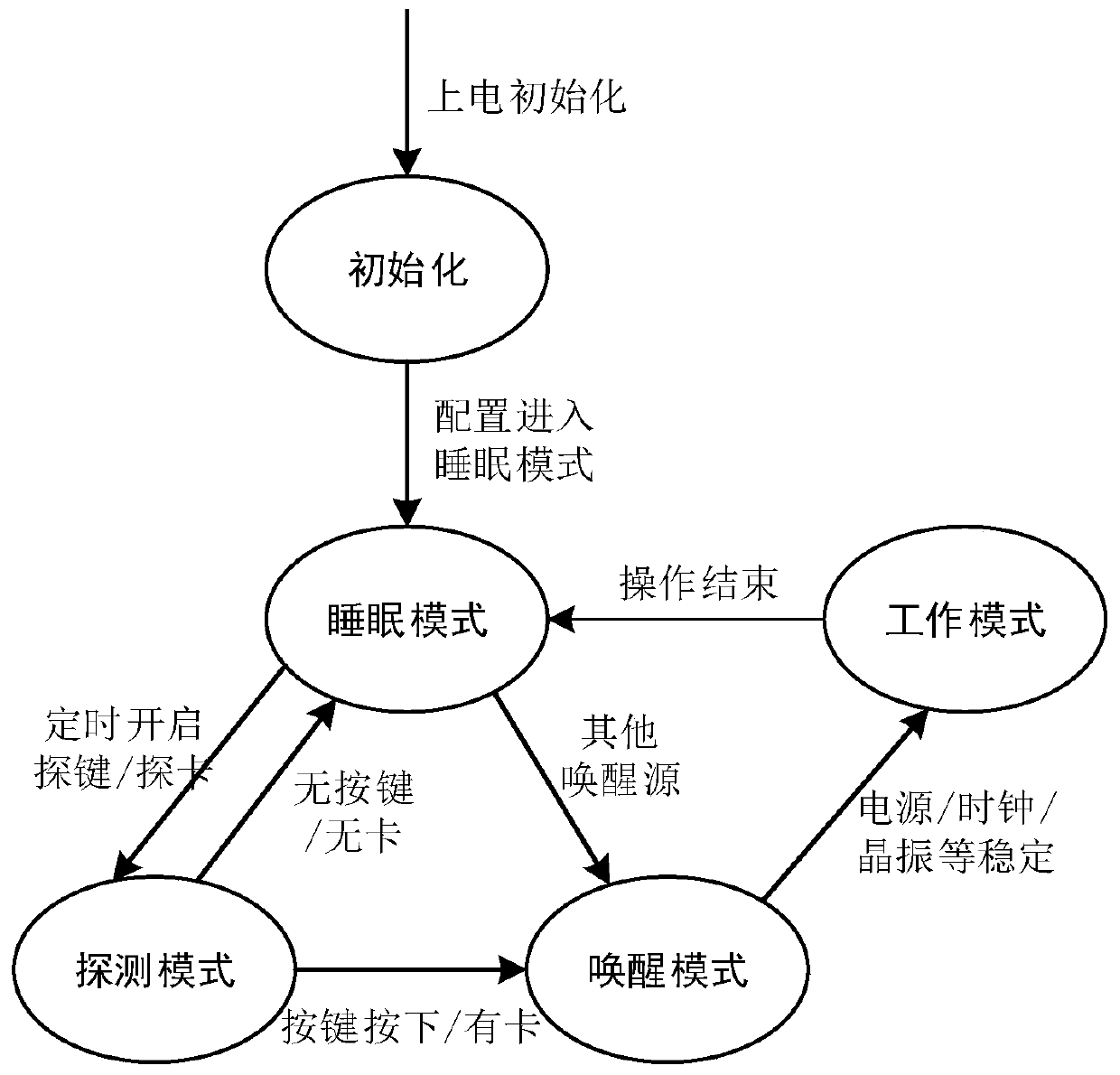
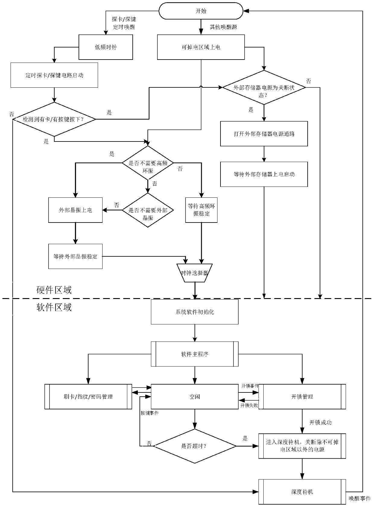
[0005] The present invention provides a low-power chip architecture system and a quick startup method with multiple wake-up source inputs. The power supply of each circuit is controlled by the power management circuit, and the high-frequency ring vibration is used as the clock of the main circuit to start, waiting for the crystal oscillator After the output precise clock is stable, switch back to the precise clock to process software programs that require precise clocks, so as to solve the technical problems of slow startup and high power consumption of the existing smart lock chip, thereby speeding up the startup of the chip and the operation of the program and reducing the cost of the chip. power consumption

Method used


Image

  • Multi-wake-up-source input low-power-consumption chip architecture system and quick starting method
  • Multi-wake-up-source input low-power-consumption chip architecture system and quick starting method
  • Multi-wake-up-source input low-power-consumption chip architecture system and quick starting method

Examples


Embodiment Construction

[0037] The following will clearly and completely describe the technical solutions in the embodiments of the present invention with reference to the accompanying drawings in the embodiments of the present invention. Obviously, the described embodiments are only some of the embodiments of the present invention, not all of them. Based on the embodiments of the present invention, all other embodiments obtained by persons of ordinary skill in the art without creative efforts fall within the protection scope of the present invention.

[0038] Please refer to Figure 1 to Figure 3 , a preferred embodiment of the present invention provides a low-power chip architecture system with multiple wake-up source inputs, including: a power management circuit, a wake-up logic circuit, a timing detection circuit, a low-frequency clock, a main circuit, a clock selector, and a high-frequency ring oscillator;

[0039] The power management circuit is used to control the power input of the wake-up lo...


PUM


Abstract

The invention discloses a low-power-consumption chip architecture system with multiple wake-up source inputs. The low-power-consumption chip architecture system comprises a power management circuit, awake-up logic circuit, a timing detection circuit, a low-frequency clock, a main circuit, a clock selector and a high-frequency ring oscillator, the power supply management circuit is used for controlling the power supply input of each circuit to open or close; the wake-up logic circuit is used for acquiring a wake-up signal sent by the timing detection circuit module and sending a correspondingcontrol signal to the power supply management circuit; the timing detection circuit is used for detecting an external wake-up signal to judge a trigger action and sending the wake-up signal to the wake-up logic circuit; the low-frequency clock circuit is used for providing a working clock for the awakening logic circuit and the timing detection circuit; wherein the main circuit is used for processing data and is connected with the awakening logic circuit through a communication port; the clock selector is used for selecting a high-frequency ring oscillator or an external crystal oscillator clock as a clock input into the main circuit; and the high-frequency ring oscillation circuit is used for providing frequencies of multiple gears for the main circuit to use.

Description

technical field [0001] The invention relates to the field of low power consumption circuits, in particular to a low power consumption chip architecture system with multiple wake-up source inputs and a quick start method. Background technique [0002] With the continuous development of smart locks, it is no longer limited to one way to open the door, and gradually develops in the direction of the coexistence of multiple door opening methods, such as the simultaneous support of button password opening, RFID card swiping, fingerprint recognition, and face recognition. Wait. If the functional circuits implemented by each door opening method are to be integrated into one chip, it is necessary to meet all the design requirements of various functional circuits, and it is necessary to consider that the chip can selectively turn off unnecessary ones in different application scenarios. functional circuit. Different door opening methods have different design requirements for chip des...

Claims


Application Information

Patent Timeline
IPC IPC(8): G06F1/3234
CPCG06F1/3234
Inventor 罗聪胡胜发
Owner ANYKA (GUANGZHOU) MICROELECTRONICS TECH CO LTD
Learn More