Static random access memory based on back gate structure of FDSOI device

A static random access and memory technology, applied in static memory, digital memory information, information storage, etc., can solve the problem of reducing the yield of SRAM

Pending Publication Date: 2020-05-12
EAST CHINA NORMAL UNIV +1
View PDF4 Cites 6 Cited by
  • Summary
  • Abstract
  • Description
  • Claims
  • Application Information

AI Technical Summary

Problems solved by technology

[0003] After the process is scaled down to the deep nano-node, the impact of process fluctuations, mainly including random doping fluctuations, oxide layer thickness fluctuations, and edge roughness fluctuations on the scribe line, on the stability of data in SRAM cannot be ignored, which greatly reduces the Yield of SRAM

Method used


Image

  • Static random access memory based on back gate structure of FDSOI device
  • Static random access memory based on back gate structure of FDSOI device
  • Static random access memory based on back gate structure of FDSOI device

Examples


Embodiment Construction

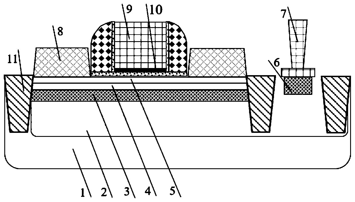
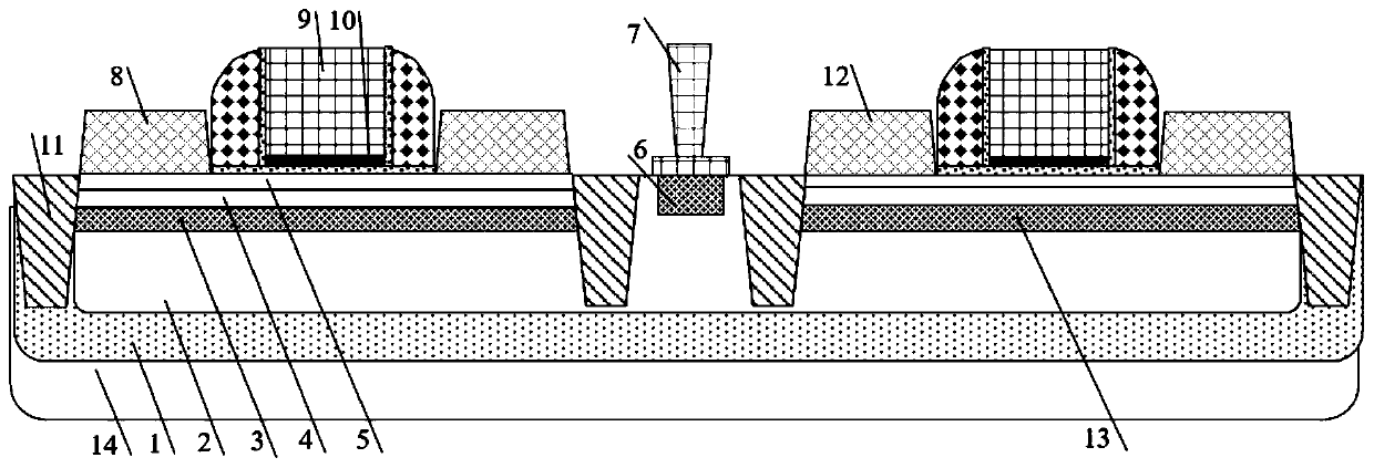
[0027] The present invention will be described in detail below in conjunction with the accompanying drawings and embodiments.

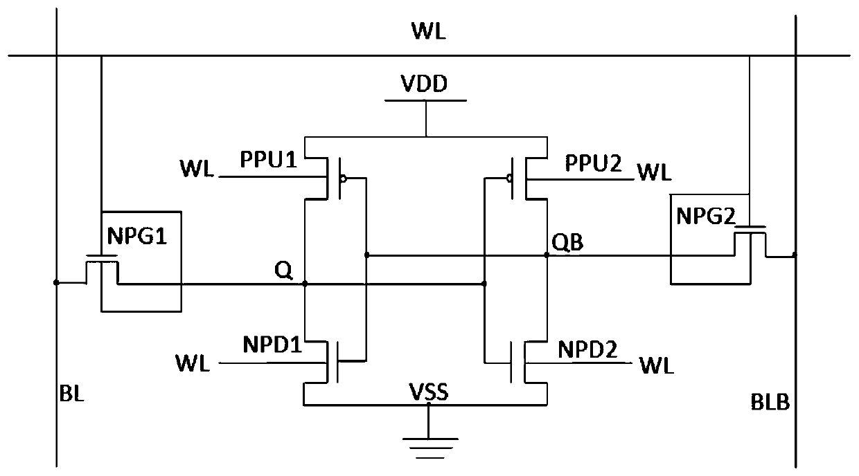
[0028] refer to figure 1 , the static random access memory of the present invention comprises:

[0029] The first pull-up transistor PPU1, the second pull-up transistor PPU2, the first pass transistor NPG1, the second pass transistor NPG2, the first pull-down transistor NPD1 and the second pull-down transistor NPD2, the first pull-up transistor PPU1, the second The pull-up transistor PPU2, the first pass transistor NPG1, the second pass transistor NPG2, the first pull-down transistor NPD1 and the second pull-down transistor NPD2 are FDSOI devices; the first pull-up transistor PPU1 and the first pull-down transistor NPD1 constitute the first An inverter, the second pull-up transistor PPU2 and the second pull-down transistor NPD2 form a second inverter;

[0030] The output terminal of the first inverter forms a first storage node Q, the output termina...


PUM


Abstract

The invention discloses a static random access memory (SRAM) based on a back gate structure of a FDSOI device, all transistors on the novel static random access memory are FDSOI devices, and back gates of the devices are connected with a word line WL. When the SRAM performs read-write operation, the word line is at a high level, so that the threshold voltage of the PMOS is increased, and the threshold voltage of the NMOS is reduced, thereby enhancing the write-in capability of the SRAM and improving the read current; in the maintaining state, the word line WL is at a low level, and the threshold voltage of the device on the SRAM is not different from the threshold voltage of the device on the traditional FDSOI SRAM, so that the static power consumption is not changed.

Description

technical field [0001] The invention belongs to the technical field of CMOS very large integrated circuits (VLSI), and in particular relates to a static random access memory based on the back gate structure of an FDSOI device. Background technique [0002] Static random access memory (SRAM) is widely used in microprocessors and SoC chips due to its advantages of saving information without refreshing, stable data storage, fast read and write speed, and low power consumption. In order to obtain better performance, in microprocessors and SoC systems, the area occupied by memory continues to increase. According to the International Technology Roadmap For Semiconductors (ITRS), it is predicted that more than 90% of the entire SoC chip will be in the future. area is occupied by memory. Therefore, as the SRAM storage unit occupying the largest area in the SoC chip, its power consumption, stability and area size affect various performance indicators of the entire chip, and thus gra...

Claims


Application Information

Patent Timeline
Patent Type & Authority Applications(China)
IPC IPC(8): G11C11/418G11C11/419
CPCG11C11/418G11C11/419
Inventor 赵彤王昌锋田明孙亚宾李小进石艳玲廖端泉曹永峰
Owner EAST CHINA NORMAL UNIV
Why Eureka
Try Eureka