Silicon-based substrate, substrate base plate and manufacturing method thereof, and photoelectric device

A substrate substrate and substrate technology, applied in the field of electronic technology applications, can solve problems such as lattice mismatch, difficulty in forming silicon-based substrates of group III and V materials, and the like

Inactive Publication Date: 2020-05-12
HUAWEI TECH CO LTD +1
View PDF5 Cites 5 Cited by
  • Summary
  • Abstract
  • Description
  • Claims
  • Application Information

AI Technical Summary

Problems solved by technology

[0004] However, there are problems such as lattice mismatch and anti-phase domains between the silicon (100) crystal plane and the III-V material, which makes the formation of the III-V material on the silicon-based substrate with the silicon (100) crystal plane extremely difficult.

Method used


Image

  • Silicon-based substrate, substrate base plate and manufacturing method thereof, and photoelectric device
  • Silicon-based substrate, substrate base plate and manufacturing method thereof, and photoelectric device
  • Silicon-based substrate, substrate base plate and manufacturing method thereof, and photoelectric device

Examples


Embodiment Construction

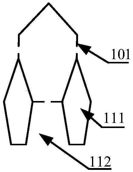
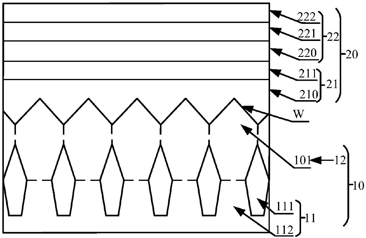
[0086] The embodiments of the present application relate to the improvement of silicon-based substrates and base substrates manufactured based on the silicon-based substrates. Silicon belongs to the cubic crystal system. In the embodiments of the present application, silicon wafers with multiple crystal faces are involved. 100) Silicon wafers with crystal planes, silicon wafers with silicon (110) crystal planes, and silicon wafers with silicon (111) crystal planes. In order to facilitate readers' understanding, these silicon wafers are introduced as follows:

[0087] A silicon wafer with a silicon (100) crystal plane is also called a silicon wafer (100), [100] is the crystal orientation index, and the normal of the silicon (100) crystal plane is parallel to the [100] crystal orientation, that is to say (100) ) The crystal plane is perpendicular to the [100] crystal direction.

[0088] A silicon wafer with a silicon (110) crystal plane is also called a silicon wafer (110). [110] is ...


PUM

PropertyMeasurementUnit
thicknessaaaaaaaaaa
thicknessaaaaaaaaaa
thicknessaaaaaaaaaa

Abstract

The invention relates to a silicon-based substrate, a substrate base plate and a manufacturing method thereof, and a photoelectric device, and relates to the field of electronic technology application. The substrate base plate comprises: a silicon-based substrate, wherein one surface of the silicon-based substrate is provided with periodic convex structures, and inclination angles are formed at the side surfaces and the bottom surfaces of each convex structure; and an III-V material layer arranged on one surface, having the convex structure, of the silicon-based substrate. According to the invention, in the substrate base plate, one surface of the silicon-based substrate is not a silicon (100) crystal surface any more and is a periodic convex structure, the self-annihilation of dislocationcan be realized by the convex structure, and dislocation caused by lattice mismatch and a reversed phase domain is limited on the silicon-based substrate layer, so that the neat crystal structure canbe kept when the III-V material epitaxially grows on the silicon-based substrate so as to reduce the problems of lattice mismatch, inverse domain and the like between the silicon-based substrate andthe III-V material and improve the yield of the III-V material on the silicon-based substrate; and the method is used for forming the high-quality III-V material on the silicon-based substrate.

Description

Technical field [0001] The present disclosure relates to the application field of electronic technology, in particular to a silicon-based substrate, a base substrate and a manufacturing method thereof, and a photoelectric device. Background technique [0002] Silicon-based optoelectronic integration technology refers to the technology of integrating optoelectronic devices on a silicon-based substrate. Devices such as light sources, amplifiers or modulators formed by this technology have the advantages of low cost, micro size and high integration. [0003] However, because silicon is an indirect bandgap material, it has poor light-emitting properties, and the third and fifth group (also called III-V group) materials have excellent optical properties. Therefore, the preparation of the third and fifth group materials on a silicon-based substrate can form Efficient light-emitting devices provide a good foundation for the formation of optoelectronic devices. For example, the third and...

Claims


Application Information

Patent Timeline
Patent Type & Authority Applications(China)
IPC IPC(8): H01L33/22H01L33/00H01L33/06H01L33/12H01L33/16H01L33/30
CPCH01L33/22H01L33/16H01L33/06H01L33/305H01L33/12H01L33/0066H01L33/30C30B29/42C30B23/025C30B25/04H01L33/20H01L21/02631H01L21/02546H01L21/02381H01L21/0243H01L21/02433H01L21/0245H01L21/02463H01L21/02502H01L21/02507H01L21/02658H01S5/021Y02P70/50
Inventor 赵壮刘磊乐阮平王霆张建军
Owner HUAWEI TECH CO LTD
Why Eureka
Try Eureka