Three-node overturning resistant D latch for high-frequency circuit application

A technology of high-frequency circuits and latches, applied in logic circuits, power reduction of field effect transistors, electrical components, etc., can solve problems such as multiple hardware, large transmission delay, and cost

Inactive Publication Date: 2020-05-12
ZHONGBEI UNIV
View PDF0 Cites 0 Cited by
  • Summary
  • Abstract
  • Description
  • Claims
  • Application Information

AI Technical Summary

Problems solved by technology

[0004] The present invention aims to solve the problems that the traditional anti-three-node flipping D latch requires more hardware, high power consumption, long transmission path, and large transmission delay. Three-node Flip D-Latch

Method used


Image

  • Three-node overturning resistant D latch for high-frequency circuit application
  • Three-node overturning resistant D latch for high-frequency circuit application
  • Three-node overturning resistant D latch for high-frequency circuit application

Examples


Embodiment Construction

[0058] The technical solutions in the embodiments of the present invention will be clearly and completely described below with reference to the accompanying drawings in the embodiments of the present invention. Obviously, the described embodiments are only a part of the embodiments of the present invention, but not all of the embodiments. Based on the embodiments of the present invention, all other embodiments obtained by those of ordinary skill in the art without creative work fall within the protection scope of the present invention.

[0059] It should be noted that the embodiments of the present invention and the features of the embodiments may be combined with each other under the condition of no conflict.

[0060] The present invention will be further described below with reference to the accompanying drawings and specific embodiments, but it is not intended to limit the present invention.

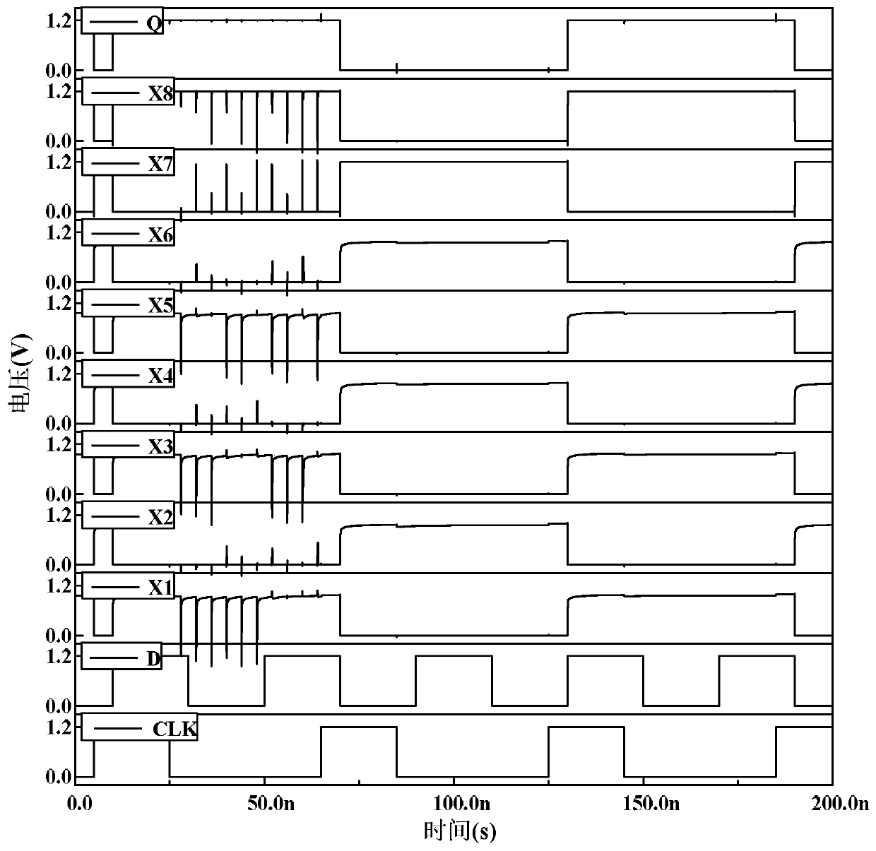
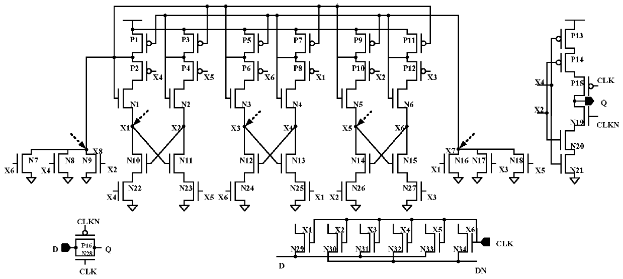
[0061] see figure 1 Illustrating this embodiment, the anti-three-node inversion ...


PUM


Abstract

The invention discloses a three-node overturning resistant D latch for high-frequency circuit application, and belongs to the field of anti-nuclear reinforcement in integrated circuit reliability. Theproblems that a traditional D latch resisting three-node overturning needs to consume more hardware, and is high in power consumption, long in transmission path and large in transmission delay are solved. The D latch comprises 34 NMOS transistors N1 to N34 and 16 PMOS transistors P1 to P16, according to the invention, the NMOS transistors are connected in series and stacked for construction, thestacking mode can effectively reduce the problem of electric leakage caused by threshold loss, and protection of quick recovery of three-node overturning is realized. And some nodes are connected by adopting a principle of nearby connection, so that connected metal wires are shorter and symmetrical, the layout area is small, and the communication performance is better and the recovery time is shorter. The invention is mainly applicable to high-frequency circuits.

Description

technical field [0001] The invention belongs to the field of anti-nuclear reinforcement in integrated circuit reliability. Background technique [0002] As the feature size of the device decreases, the junction capacitance of the device decreases, the operating voltage decreases, and the single-event critical charge decreases. more sensitive. [0003] Due to the changes in the material, structure and size of nanodevices, the coupling relationship between the single-event effect and circuit logic is also more complex, and phenomena such as obvious single-event crosstalk and multi-node charge collection appear. For multi-node charge collection caused by a single particle, the node directly hit by the particle is usually called the active node, the node indirectly affected by the charge diffusion generated by the single particle is called the passive node, and the active node charge affects the passive node through charge diffusion. The process of nodes is called charge shari...

Claims


Application Information

Patent Timeline
Patent Type & Authority Applications(China)
IPC IPC(8): H03K19/003H03K19/00H03K19/017
CPCH03K19/0013H03K19/0016H03K19/00315H03K19/00338H03K19/01728
Inventor 杜芳芳郭靖
Owner ZHONGBEI UNIV
Why Eureka
Try Eureka