Overlay deviation determination method and system

A technology of overlay deviation and determination method, which is applied in the field of overlay deviation determination method and system, can solve problems such as uneven stress distribution, reduced wafer yield, and no solution is proposed, so as to save process cost and product technology. Stable and accurate, the effect of improving product yield

Active Publication Date: 2020-05-15
YANGTZE MEMORY TECH CO LTD
View PDF9 Cites 2 Cited by
  • Summary
  • Abstract
  • Description
  • Claims
  • Application Information

AI Technical Summary

Problems solved by technology

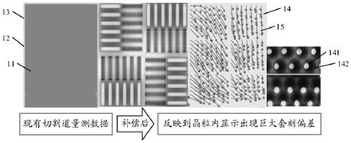
However, as the number and thickness of the device continue to increase, the stress distribution between the center and edge of the wafer, each exposure area (Shot) and each die (Die) will become uneven
At this time, there will be a significant difference between the conditions in the scribe line and the grain, and the overlay mark on the scribe line alone cannot accurately reflect the actual situation of the overlay deviation in the die. If the overlay mark on the scribe line is still used for measurement and Compensation, there will be a great risk of compensating the alignment accuracy of the overlay in the die to be worse, which will have a great impact on the stability of the lithography process and product process, which will lead to a serious decrease in the yield of the wafer
[0004] For the above-mentioned problems existing in related technologies, no effective solution has been proposed yet

Method used


Image

  • Overlay deviation determination method and system
  • Overlay deviation determination method and system
  • Overlay deviation determination method and system

Examples


Embodiment Construction

[0024] In order to make the purpose, technical solution and advantages of the application more clear, the technical solution of the application will be further elaborated below in conjunction with the accompanying drawings and embodiments. The described embodiments should not be considered as limiting the application. All other embodiments obtained under the premise of no creative work belong to the scope of protection of this application.

[0025] In the following description, references to "some embodiments" describe a subset of all possible embodiments, but it is understood that "some embodiments" may be the same subset or a different subset of all possible embodiments, and Can be combined with each other without conflict.

[0026] If there is a similar description of "first / second" in the application documents, add the following explanation. In the following description, the terms "first\second\third" are only used to distinguish similar objects, not Represents a specific...


PUM


Abstract

The embodiment of the invention discloses an overlay deviation determination method and system, wherein the method comprises the steps of setting an overlay mark along the central part of a side boundary in a unit array region during a process of carrying out the photoetching technology on each layer of wafer and in each crystal grain on a photomask pattern; and when the overlay alignment operation is carried out, measuring the overlay mark of the current layer and the overlay mark of the previous layer of the current layer through a measuring device, and determining the overlay deviation of the current layer and the previous layer.

Description

technical field [0001] The present application relates to but not limited to the field of semiconductor manufacturing, and in particular relates to a method and system for determining an overlay deviation. Background technique [0002] Three-dimensional NAND (3D NAND) memory is currently a popular device in the field of semiconductor memory. It adopts a device structure of vertically stacked multi-layer memory cells, which reduces the unit cost of memory cells while achieving extremely high data storage density. Due to the multi-layer stacking of the device structure, multi-layer photolithography and alignment are required during the process of the 3D NAND memory. [0003] In the related art, in order to monitor the overlay (Overlay, OVL) alignment accuracy of each layer process, the overlay mark is placed on the cutting line for measurement to realize the monitoring of the product process, and the overlay is adjusted according to the measured overlay deviation value. The e...

Claims


Application Information

Patent Timeline
Patent Type & Authority Applications(China)
IPC IPC(8): G03F7/20
CPCG03F7/70633H01L23/544H01L22/12H01L22/20H01L2223/54426Y02P70/50
Inventor 郭芳芳陆聪李伟卢绍祥轩攀登
Owner YANGTZE MEMORY TECH CO LTD
Why Eureka
Try Eureka