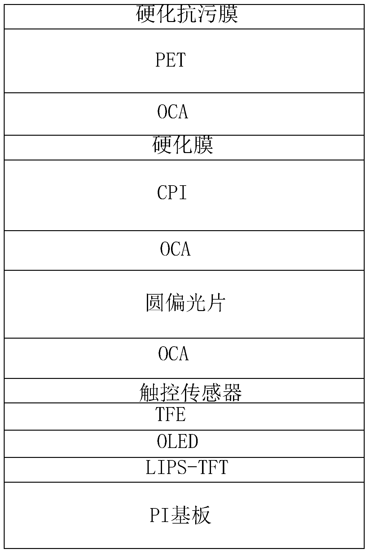
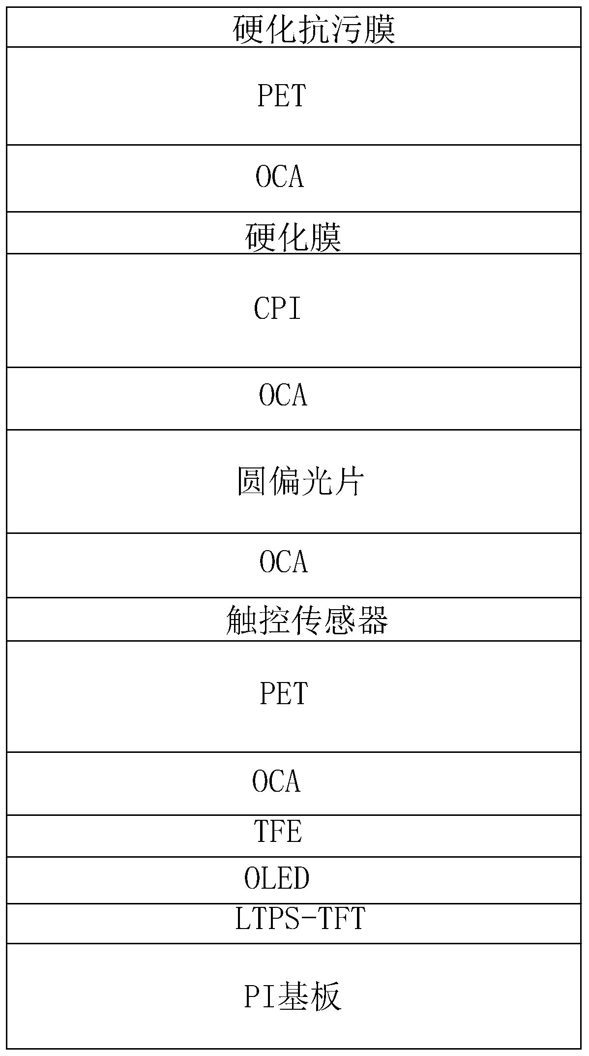
Structure and manufacturing method of foldable AMOLED display screen
A manufacturing method and display technology, applied in the input/output process of data processing, instruments, electrical digital data processing, etc., can solve the problems of unfavorable folding screens, increased thickness, creases, etc., and achieve good folding recovery and overall The effect of thickness reduction and yield improvement
- Summary
- Abstract
- Description
- Claims
- Application Information
AI Technical Summary
Problems solved by technology
Method used
Image
Examples
Embodiment 1
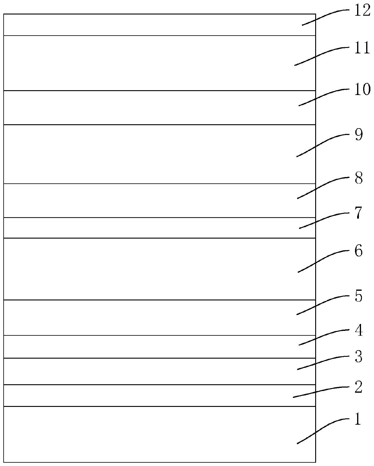
[0060] Such as image 3 As shown, a foldable AMOLED display structure includes a PI substrate 1, a circuit driving layer 2, and an OLED layer 3 from bottom to top, and a multi-layer thin film encapsulation layer 4 is arranged above the OLED layer 3, and the multi-layer thin film An ultra-thin glass layer 6 is pasted on the packaging layer, a touch sensor layer 7 is coated on the top of the ultra-thin glass layer 6, a circular polarizer 9 is pasted on the top of the touch sensor layer 7, and PET11, PET11 is pasted on the top of the circular polarizer The upper surface is provided with a hardened antifouling film 12 .
[0061] The circuit driving layer in this embodiment is a TFT made of LTPS, the OLED layer is RGB_OLED, and the TFT and OLED form an AMOLED.
[0062] This embodiment preferably also includes a first optical adhesive layer 5, a second optical adhesive layer 8, and a third optical adhesive layer 10, and the ultra-thin glass layer and the multilayer film packaging l...
Embodiment 2
[0077] Such as Figure 4 As shown, a foldable AMOLED display structure includes a PI substrate 1, a circuit driving layer 2, and an OLED layer 3 from bottom to top, and a multi-layer thin film encapsulation layer 4 is arranged above the OLED layer 3, and the multi-layer thin film A circular polarizer 9 is pasted on the top of the encapsulation layer 4, an ultra-thin glass layer 6 is pasted on the top of the circular polarizer 9, a touch sensor layer 7 is coated on the top of the ultra-thin glass layer 6, and a touch sensor layer 7 is coated on the top of the touch sensor layer 7. Laminated with PET11, the upper surface of the PET is provided with a hardened antifouling film 12.
[0078] In this embodiment, the first optical adhesive layer 5 is used to bond the circular polarizer and the multilayer thin film encapsulation layer; the second optical adhesive layer 8 is used to bond the circular polarizer and the ultra-thin glass layer; the third optical adhesive layer 10 Used fo...
PUM
| Property | Measurement | Unit |
|---|---|---|
| thickness | aaaaa | aaaaa |
| thickness | aaaaa | aaaaa |
| thickness | aaaaa | aaaaa |
Abstract
Description
Claims
Application Information


