
Epitaxial layer material stripping method based on 3D laminated mask substrate

An epitaxial layer and mask layer technology, applied in the field of optoelectronics, can solve the problems of slow grinding and polishing rate, unfavorable production efficiency, yield drop, etc., and achieve the effects of improving efficiency, low cost and high yield

Active Publication Date: 2020-05-22
北京飓芯科技有限公司
View PDF9 Cites 4 Cited by
  • Summary
  • Abstract
  • Description
  • Claims
  • Application Information

AI Technical Summary

Problems solved by technology

[0018] a) A certain amount of mechanical stress will be generated during the grinding and polishing process, especially when it is already relatively thin, the mechanical stress may break the material, resulting in a decrease in yield
[0019] b) Both sapphire and silicon carbide are relatively hard materials, and their hardness is second only to diamond, so the grinding and polishing rate is very slow, and the mechanical force used will be greater. It takes several hours to complete the grinding and polishing of a sapphire substrate. Therefore, it is not conducive to the improvement of production efficiency

Method used


Image

  • Epitaxial layer material stripping method based on 3D laminated mask substrate
  • Epitaxial layer material stripping method based on 3D laminated mask substrate
  • Epitaxial layer material stripping method based on 3D laminated mask substrate

Examples


Embodiment Construction

[0052] In order to make the above objects, features and advantages of the present invention more comprehensible, the present invention will be further described in detail below through specific embodiments and accompanying drawings.

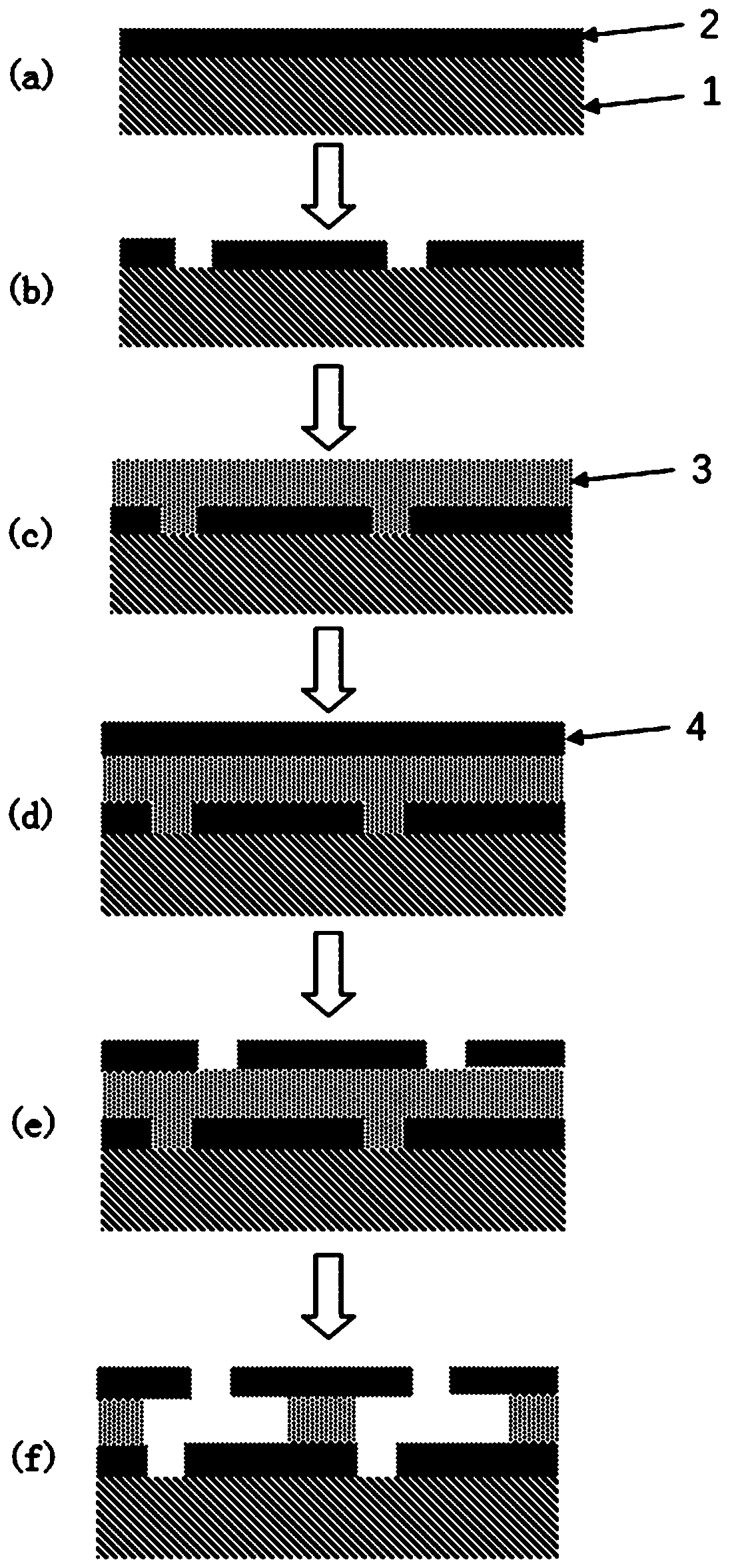
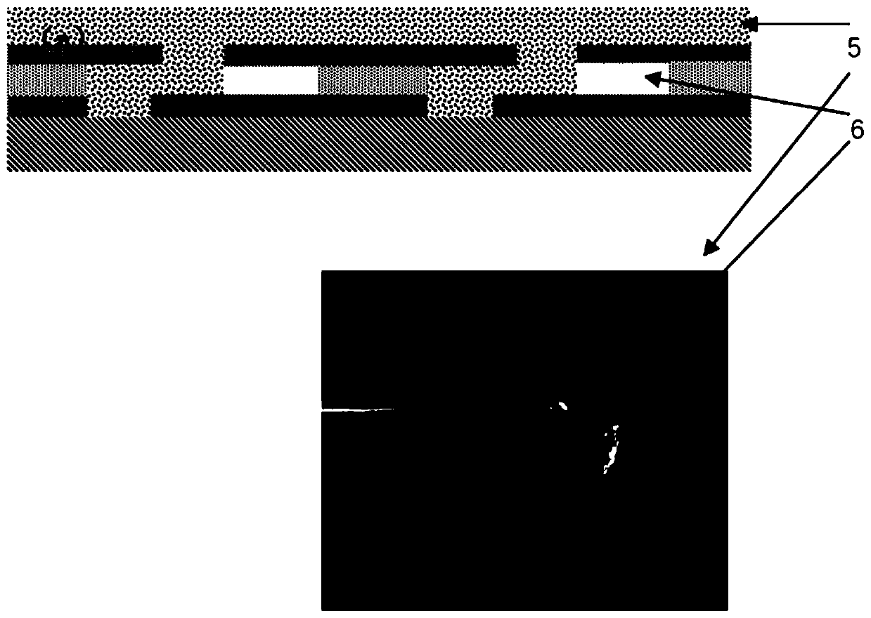
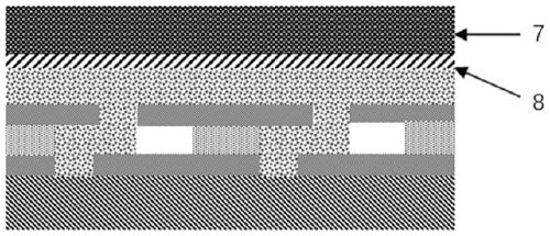
[0053] The core of the technical solution of the present invention lies in the combination of graphic substrate structure design and wet etching process. In terms of substrate structure design, the new 3D laminated substrate technology is mainly adopted. In this technology, the graphic positions of the upper and lower masks are offset from each other. After the etching process, the connection between the upper and lower mask windows is opened, so that GaN can be grown meandering from the bottom window and eventually drilled out of the top window. Such as figure 1 As shown, it specifically includes the following steps:

[0054] 1) Deposit the underlying mask layer 2 (first layer mask) on the substrate 1, such as figure 1 As shown in (a) figure....


PUM


Abstract

The invention discloses an epitaxial layer material stripping method based on a 3D laminated mask substrate, is used for epitaxial growth and stripping of III-V group compound semiconductor materialssuch as GaN, and belongs to the technical field of photoelectrons. The substrate structure comprises a substrate, wherein a bottom mask layer, a middle layer and a top mask layer are sequentially arranged on the substrate; the window of the bottom mask layer and the window of the top mask layer are mutually staggered. The invention also provides a preparation method of the substrate structure andan epitaxial layer stripping method based on the substrate structure. Compared with the prior art, the invention provides a more optimized peelable method, the peeling success rate is improved, the peeling time is shortened, and the peelable method has higher use value.

Description

technical field [0001] The invention belongs to the field of optoelectronic technology, and in particular relates to a method for stripping epitaxial layer materials based on a 3D stacked mask substrate, which is used for epitaxial growth and stripping of III-V compound semiconductor materials such as GaN. Background technique [0002] At present, the third-generation semiconductor materials represented by gallium nitride (GaN) have been widely used in many important fields, such as semiconductor lasers, early warning aircraft radars, and fast chargers. Due to the lack of homogeneous substrates, most GaN materials are grown epitaxially using heterogeneous substrates, such as single crystal substrates such as sapphire, silicon, and silicon carbide. These heterogeneous substrates have large lattice and thermal mismatches with the GaN material, thus accumulating stress. In order to obtain a stress-free GaN material, it is necessary to lift the GaN material from the foreign sub...

Claims


Application Information

Patent Timeline
Patent Type & Authority Applications(China)
IPC IPC(8): H01L21/78H01L21/311
CPCH01L21/7813H01L21/31111
Inventor 张晓蓉郑烨琳冯筱陈明兰
Owner 北京飓芯科技有限公司
Learn More