Quantum dot LED packaging device and manufacturing method thereof

A technology of LED packaging and manufacturing methods, which is applied to semiconductor devices, electrical components, circuits, etc., can solve problems such as poor water and oxygen stability, low yield and yield, and poor device adaptability, so as to reduce failure, improve utilization rate, and improve The effect of stability

Pending Publication Date: 2020-05-22
SHINEON BEIJING TECH
View PDF0 Cites 2 Cited by
  • Summary
  • Abstract
  • Description
  • Claims
  • Application Information

AI Technical Summary

Problems solved by technology

[0003] However, the existing quantum dot materials have poor water and oxygen stability, short life and rapid failure under conventional packaging, and ordinary packaging methods cannot achieve effective protection of materials. The existing quantum dot applications only stay at the diaphragm stage, and the amount of materials used is large. , poor device adaptability, and low yield and yield

Method used


Image

  • Quantum dot LED packaging device and manufacturing method thereof
  • Quantum dot LED packaging device and manufacturing method thereof
  • Quantum dot LED packaging device and manufacturing method thereof

Examples


Embodiment Construction

[0037] In order to make the purpose, technical solutions and advantages of the embodiments of the present invention clearer, the technical solutions in the embodiments of the present invention will be clearly and completely described below in conjunction with the drawings in the embodiments of the present invention. Obviously, the described embodiments It is a part of the embodiments of the present invention, but not all of them. Based on the embodiments of the present invention, all other embodiments obtained by those of ordinary skill in the art without creative work belong to the protection of the present invention. scope.

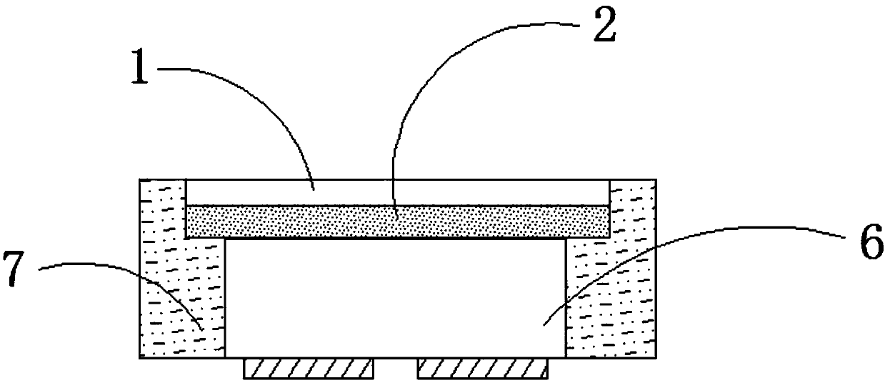
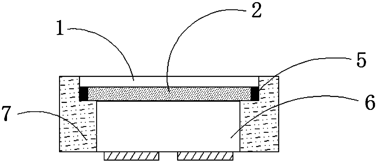
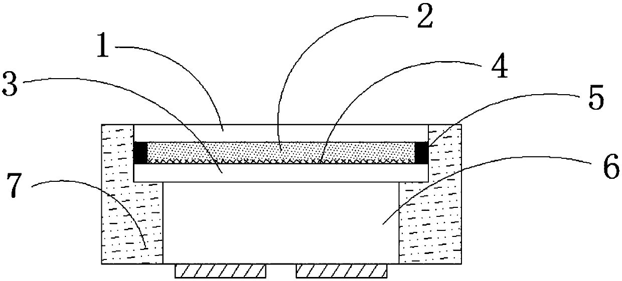
[0038] Such as figure 1 As shown, the embodiment of the present invention provides a quantum dot LED packaging device, the quantum dot LED packaging device includes: upper surface glass layer 1, quantum dot layer 2, LED chip 6 and packaging material 7, quantum dot layer 2 is located on the upper Between the surface glass layer 1 and the flip-chip LED c...


PUM

PropertyMeasurementUnit
thicknessaaaaaaaaaa
thicknessaaaaaaaaaa

Abstract

The invention discloses a quantum dot LED packaging device and a manufacturing method thereof. The device mainly comprises a quantum dot material or a mixture of quantum dots and fluorescent powder which is positioned between two layers of glass, or is protected by at least upper-layer glass, epoxy resin or other protective materials which are coated on the peripheral edge between the pieces of glass, an inverted LED chip which is bonded on the lower surface of the glass layer, a film layer and water glue coated at the periphery of the inverted LED chip, wherein the water glue is used for sealing the quantum dot material into a closed cavity formed by an upper layer of glass, a lower layer of glass, epoxy resin or other protective materials, and after the lower surface of the glass is bonded to the upper surface of the flip LED chip, the periphery of the whole structure is coated with the white glue. On the basis of ensuring the light emitting uniformity, the use amount of the quantumdot material is reduced, and water and oxygen isolation sealing is realized, so that the material failure is reduced, the device stability is improved, in addition, the chip light emitting utilizationrate is improved, the light effect, the power bearing capability, the device adaptability and the service life are improved, and the cost is reduced.

Description

technical field [0001] The invention relates to the technical field of semiconductor lighting, in particular to a quantum dot LED packaging device and a manufacturing method. Background technique [0002] With the improvement of economic level, people's pursuit of high-quality life is becoming more and more urgent. The improvement of light source and display effect will make people feel more comfortable and comfortable. As a new type of luminescent material, quantum dot materials have a wide laser spectrum. , good monochromaticity, adjustable luminous wind wavelength, high conversion efficiency, can achieve precise control of the spectrum and effective improvement of the color gamut of backlight products, and has more economic advantages and application prospects compared with the current phosphor solution. [0003] However, the existing quantum dot materials have poor water and oxygen stability, short life and rapid failure under conventional packaging, and ordinary packagi...

Claims


Application Information

Patent Timeline
Patent Type & Authority Applications(China)
IPC IPC(8): H01L33/50H01L33/54H01L33/56
CPCH01L33/505H01L33/507H01L33/54H01L33/56H01L2933/005
Inventor 申崇渝张冰李德建雷利宁
Owner SHINEON BEIJING TECH
Why Eureka
Try Eureka