Cation doping device and cation doping method for metal oxide film
An oxide film, cation technology, applied in electrochemical generators, instruments, non-aqueous electrolyte battery electrodes, etc., can solve the problem of inability to further control the ion concentration distribution and control the doping area, and achieve the effect of strong universality
- Summary
- Abstract
- Description
- Claims
- Application Information
AI Technical Summary
Problems solved by technology
Method used
Image
Examples
Embodiment 1
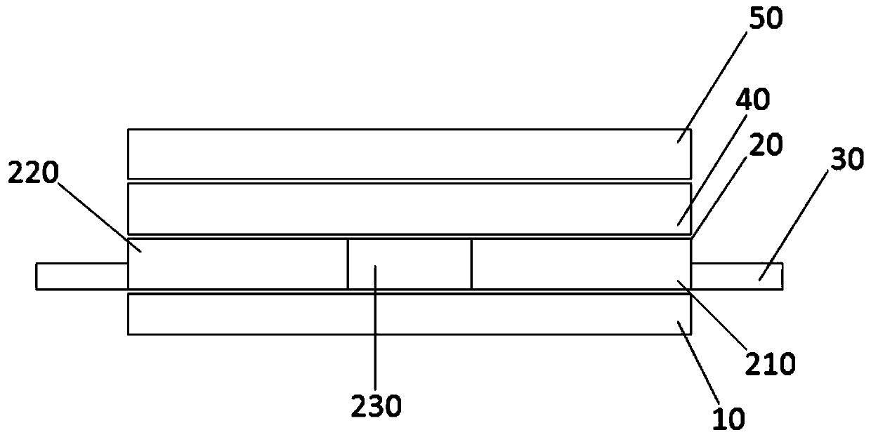
[0041] This example provides a cation doping device for a metal oxide thin film, the structure of which is as follows figure 1 shown, including
[0042] The base layer 10, and the conductive layer 20 arranged on the surface of the base layer 10, the two sides of the conductive layer 20 are provided with the electrode layer 30, the surface of the conductive layer 20 is provided with a metal oxide film 40, the metal An electrolyte layer 50 is provided on the surface of the oxide film 40;
[0043] The conductive layer 20 includes a first conductive layer 210 and a second conductive layer 220 separated from each other, and a target doping region covering layer 230 is disposed between the first conductive layer 210 and the second conductive layer 220 .
[0044] Wherein, the base layer 10 includes glass. The conductive layer 20 includes ITO thin film, AZO thin film and FTO thin film. The metal oxide thin film 40 is one of tungsten trioxide thin film, molybdenum oxide thin film, t...
Embodiment 2
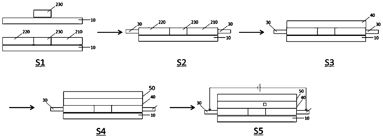
[0046] This example provides a method for cationic doping of metal oxide thin films, the steps include:
[0047] S1: taking the base layer, and setting a conductive layer on the surface of the base layer;
[0048] S2: setting electrode layers on both sides of the conductive layer;
[0049] S3: preparing a metal oxide film on the surface of the conductive layer;
[0050] S4: forming an electrolyte layer after cationic coating on the surface of the metal oxide film;
[0051] S5: Applying a doping voltage to the electrode layer, the doping voltage being an alternate forward voltage and a reverse voltage.
[0052] After the above steps are completed, the layers on the surface of the metal oxide film are removed, and the voltage is removed, so that the dopant cations stop migrating and stabilize in the metal oxide film, that is, the target doped region is permanently implanted.
[0053] In step S1, the specific method of setting a conductive layer on the surface of the base laye...
Embodiment 3
[0058] In this example, the tungsten trioxide film is doped, and the doped cation is calcium ion. The doping process is as follows: figure 2 As shown, the specific steps are as follows:
[0059] S1: Take cleaned ordinary glass as the base layer 10, stick 1cm of high-temperature glue on the middle area of the glass surface to form the target doping area covering layer 230, and then prepare an ITO film on the glass surface to form the first conductive layer 210 and the second conductive layer 220;
[0060] S2: The electrode layer 30 is prepared by sticking 0.5 cm of conductive glue on the side surfaces of the first conductive layer 210 and the second conductive layer 220, and the electrode layer 30 is only in contact with the conductive layer;
[0061] S3: preparing a tungsten trioxide film 40 on the surface of the conductive layer;
[0062] S4: preparing a liquid or gel of calcium chloride, coating it on the surface of the tungsten trioxide film 40 to form an electrolyte l...
PUM
 Abstract
Description
Claims
Application Information
 - R&D
- Intellectual Property
- Life Sciences
- Materials
- Tech Scout
- Unparalleled Data Quality
- Higher Quality Content
- 60% Fewer Hallucinations
Browse by: Latest US Patents, China's latest patents, Technical Efficacy Thesaurus, Application Domain, Technology Topic, Popular Technical Reports.
© 2025 PatSnap. All rights reserved.Legal|Privacy policy|Modern Slavery Act Transparency Statement|Sitemap|About US| Contact US: help@patsnap.com


