Wide-voltage-gain DC/DC converter for energy storage device
A technology of energy storage device and converter, which is applied in the direction of conversion equipment without intermediate conversion to AC, and can solve the problems of increasing switching loss, electromagnetic interference, and large voltage stress
- Summary
- Abstract
- Description
- Claims
- Application Information
AI Technical Summary
Problems solved by technology
Method used
Image
Examples
Embodiment 1
[0028] 1. Topology
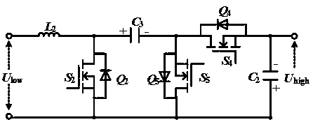
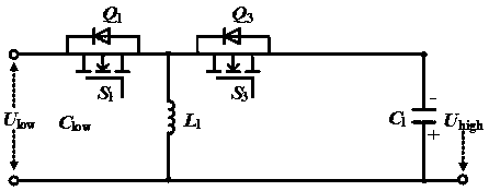
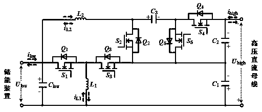
[0029] Such as image 3 Bidirectional DC / DC converter with wide voltage gain shown. The low-voltage side of the DC / DC converter is connected to the energy storage device; the high-voltage side is connected to the DC bus; the main part of the converter is composed of two traditional buck / boost converters, the first of which is as follows figure 2 shown by the inductance L 1 , power switch Q 1 , Q 3 and capacitance C 1 constitute. another such as figure 1 shown by the inductance L 2 , power switch Q 2 , Q 4 and Q 5 and capacitance C 2 and C 3 constitute. The two form a new type of bidirectional DC converter through the parallel connection of the low-voltage side and the series connection of the high-voltage side.
[0030] 2. Wide voltage gain
[0031] The present invention is divided into a boost mode and a buck mode. In the boost mode, the energy storage device provides energy for the DC bus, and the energy flows from the low volta...
Embodiment 2
[0061] Below to image 3 The novel wide voltage gain bidirectional DC / DC converter topology shown, Figure 4 , 5 , the topological equivalent circuit diagram of 7, 8 and Figure 6 and Figure 9 Important working waveforms when the topology is running stably, the principle of the scheme in the first embodiment will be described. The bidirectional is divided into boost and buck modes, and for each mode, the converter experiences two switching states in one carrier period. The two switch states in the boost mode and the buck mode are described respectively below.
[0062] boost mode
[0063] when S 1 S 2 =11, the equivalent circuit of this state is as Figure 4 As shown, the power switch tube Q 1 , Q 2 conduction, Q 3 , Q 5 anti-parallel diode reverse cut-off, Q 4 Antiparallel diodes conduct forward, according to Figure 6 Topological working waveform, low side power supply U low To inductance L 1 charging, in addition the low side power U low and C ...
PUM
 Abstract
Description
Claims
Application Information


