Bilateral multi-plane inclined wave surface interferometer and detection method thereof

A technology of wave surface interference and interferometer, which is applied in the direction of instruments, measuring devices, scientific instruments, etc., and can solve the problems of periodic in-situ calibration of errors, unsuitability for flat-panel component detection, and unsuitable detection of flat-panel component surface topography, etc.

Active Publication Date: 2020-05-29
SHANGHAI INST OF OPTICS & FINE MECHANICS CHINESE ACAD OF SCI
View PDF10 Cites 7 Cited by
  • Summary
  • Abstract
  • Description
  • Claims
  • Application Information

AI Technical Summary

Problems solved by technology

[0011] Prior technologies 6 to 10 are all oriented to the detection of aspheric and free-form surface optical components. The output light of the multiple inclined wave surface interferometer is spherical waves with different focal points, which is not suitable for detecting the surface topography of flat components; the proposed system error modeling method Standard spherical mirrors located at different positions are also used as the

Method used


Image

  • Bilateral multi-plane inclined wave surface interferometer and detection method thereof
  • Bilateral multi-plane inclined wave surface interferometer and detection method thereof
  • Bilateral multi-plane inclined wave surface interferometer and detection method thereof

Examples


Embodiment Construction

[0076] In order to better understand the purpose, technical solutions and advantages of the present invention, the present invention will be further described below in conjunction with the accompanying drawings and embodiments, but the protection scope of the present invention should not be limited thereby.

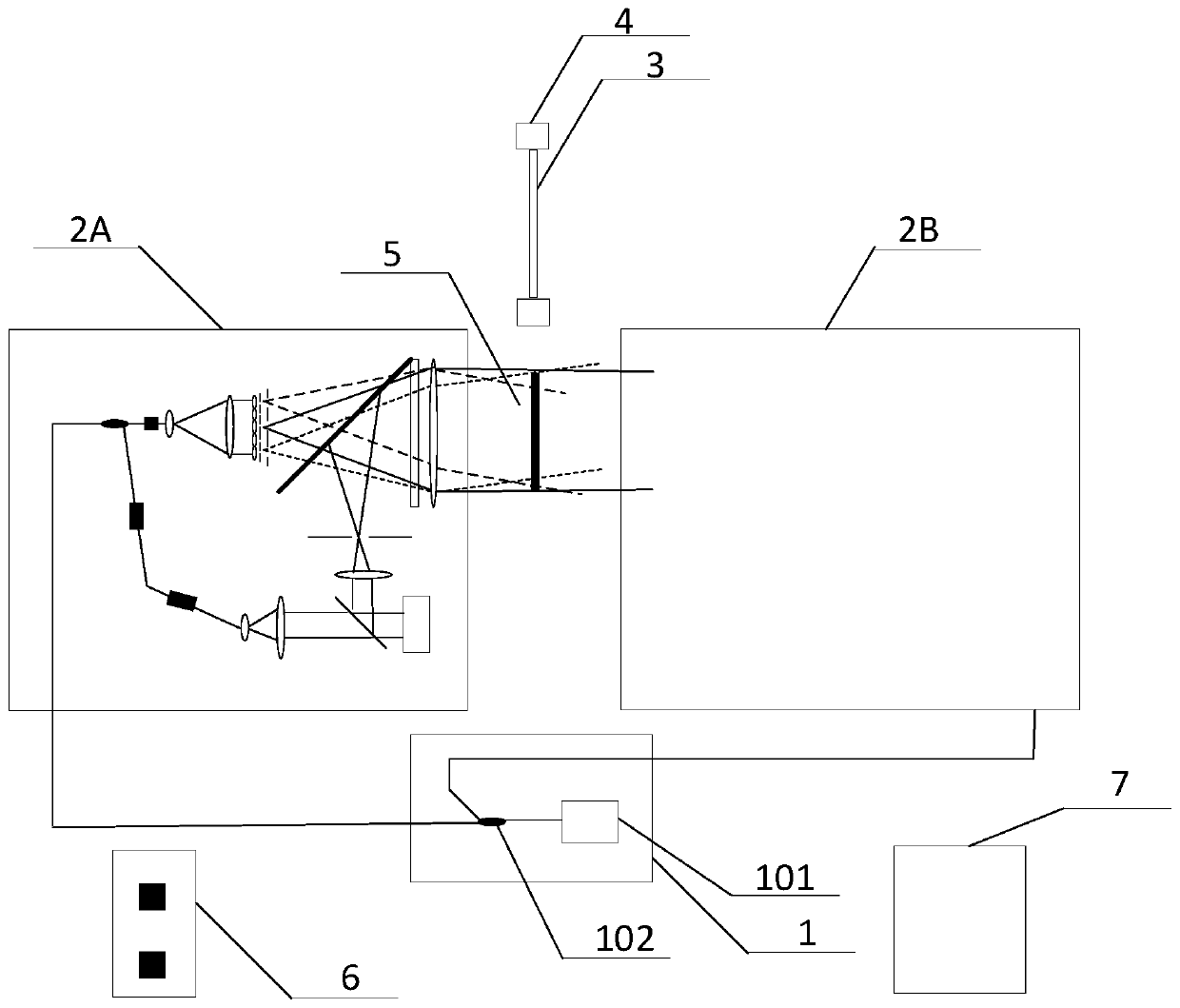
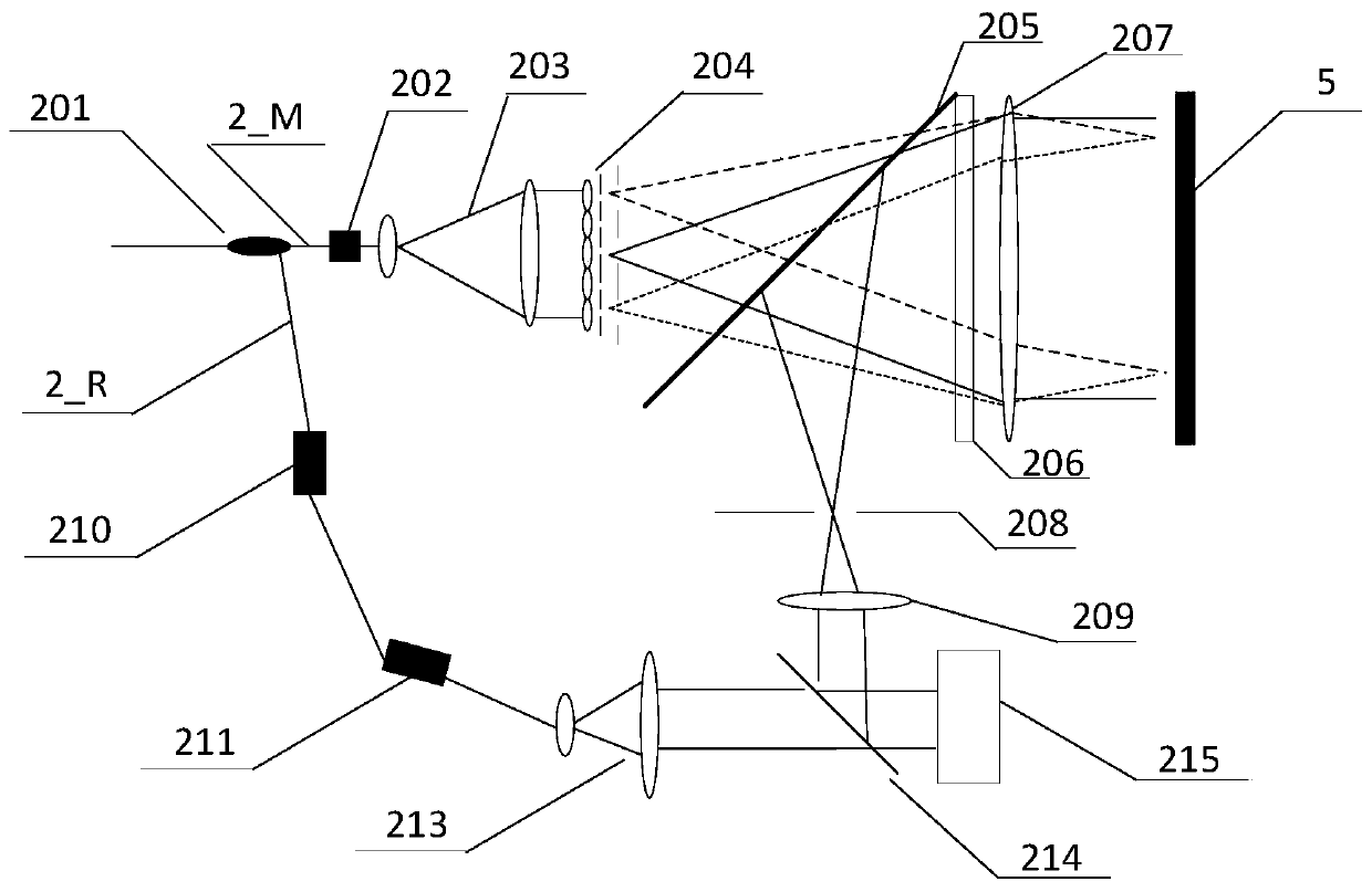
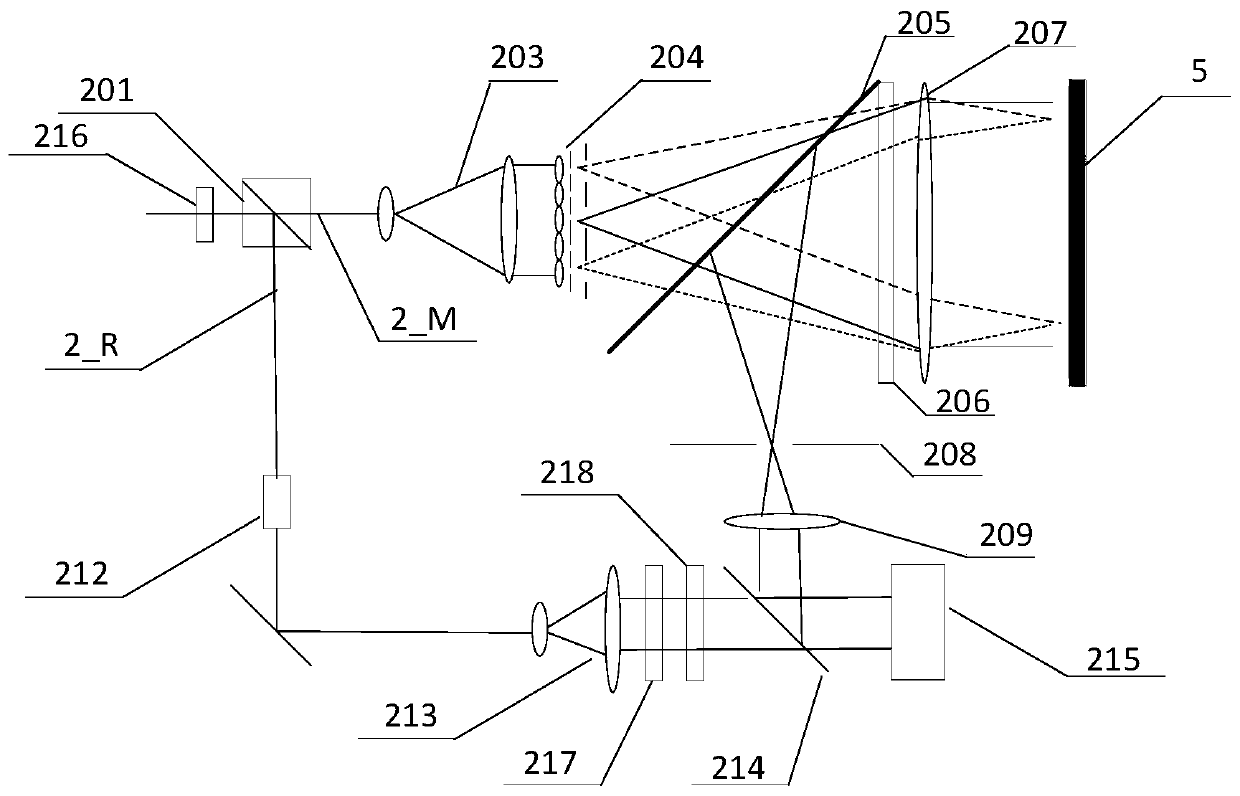
[0077] figure 1 It is a schematic diagram of the invented double-sided multi-plane inclined wave surface interferometer, the system includes a light source module 1, a first interferometer host 2A, a second interferometer host 2B, a double-sided standard plate 3, a double-sided standard plate adjustment frame 4, and a Measuring non-transparent flat plate components 5, single point thickness measuring sensor 6, control processing unit 7;

[0078] The light source module 1 outputs two paths of light, which are respectively input into the first interferometer host 2A and the second interferometer host 2B;

[0079]Both the first interferometer host 2A and the second interfer...


PUM


Abstract

The invention relates to a bilateral multi-plane inclined wave surface interferometer. The system comprises a light source module, a first interferometer host, a second interferometer host, a double-sided standard flat plate, a double-sided standard flat plate adjusting frame, a measured non-transparent flat plate element, a single-point thickness measuring sensor and a control processing unit, wherein the first interferometer host and the second interferometer host are both multi-plane inclined wave surface interferometers. The interferometer is advantaged in that parallel measurement light in multiple directions is emitted through a point source array generator to measure the bilateral morphology and thickness of the measured non-transparent flat plate element, and the interferometer hasadvantages of being large in measurement dynamic range, high in measurement precision and efficiency, flexible in phase shift mode and capable of achieving in-situ calibration of system errors.

Description

technical field [0001] The invention relates to the fields of optical measurement and semiconductor technology, in particular to a double-sided multi-plane inclined wavefront interferometer and a detection method thereof for measuring the surface topography and thickness distribution of non-transparent flat elements such as silicon wafers. Background technique [0002] Silicon wafer is an important material in the field of semiconductor technology, and it is also a special non-transparent flat optical element of visible light. Through the detection of silicon wafer shape, the stress of silicon wafer can be calculated, and the accuracy of in-plane distortion (IPD, In plane distortion) of lithographic graphics can be realized. Prediction, improve photolithographic overlay accuracy. Through the simultaneous detection of the surface topography on both sides, the thickness distribution of the silicon wafer can be obtained, which can be used for silicon wafer manufacturing, silico...

Claims


Application Information

Patent Timeline
IPC IPC(8): G01J9/02G01B11/24G01B11/06
CPCG01B11/0641G01B11/0675G01B11/2441G01J9/02G01J2009/0226G01J2009/0261
Inventor 唐锋王向朝郭福东卢云君
Owner SHANGHAI INST OF OPTICS & FINE MECHANICS CHINESE ACAD OF SCI
Why Eureka
Try Eureka