A Modulation Method of Asymmetric Ferroelectric Tunneling Junction Multi-valued Memory Cell
A technology of multi-value storage and modulation method, applied in the direction of electrical components, information storage, static memory, etc., to achieve the effect of simple method, easy process compatibility, and easy integration
- Summary
- Abstract
- Description
- Claims
- Application Information
AI Technical Summary
Problems solved by technology
Method used
Image
Examples
preparation example Construction
[0075] The present invention provides a method for preparing the above-mentioned multi-valued memory cell with asymmetric ferroelectric tunneling junction, the multi-valued memory cell comprising the above-mentioned multi-value memory cell
[0076] The method includes the following steps:
[0077] Step 1: provide a substrate, and form a first electrode layer 1 on the upper surface of the substrate;
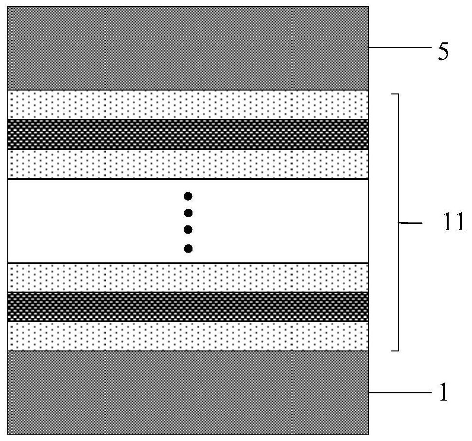
[0078] Step 2: An asymmetric ferroelectric functional layer array 11 is formed on the upper surface of the first electrode layer 1, which includes: N ferroelectric functional layers parallel to the first plane direction, two adjacent ferroelectric functional layers separated by an insulating layer;
[0079] Step 3: forming a second electrode layer 5 on the upper surface of the Nth ferroelectric functional layer;
[0080] Step 4: crystallizing the ferroelectric functional layer, so that the ferroelectric functional layer material exhibits ferroelectric properties;
[0081] In th...
Embodiment
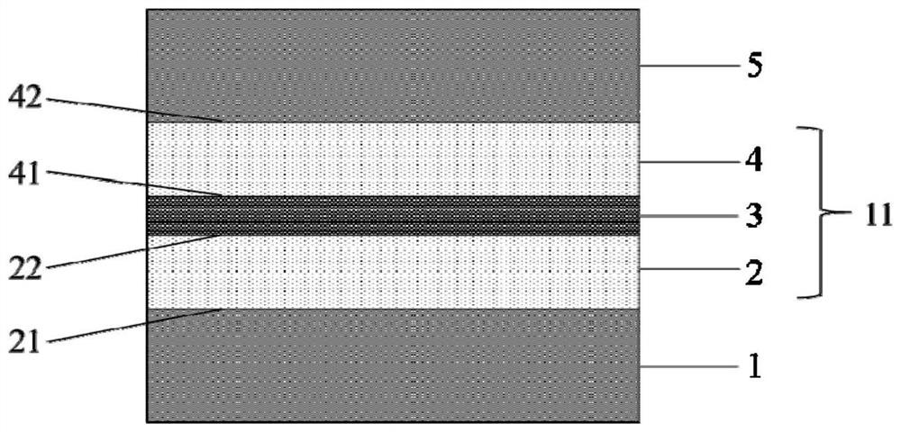
[0106] This embodiment provides a Hf-based 0.5 Zr 0.5 O 2 (hereinafter abbreviated as HZO) ferroelectric thin films and Al 2 O 3 The multi-value memory cell of asymmetric ferroelectric tunneling junction of insulating layer, its structure diagram is as follows figure 1 As shown, from bottom to top, it mainly includes a first electrode layer 1 , a first ferroelectric functional layer 2 , an insulating layer 3 , a second ferroelectric functional layer 4 , and a second electrode layer 5 . Specific steps are as follows:
[0107] (1) Preparation of the first electrode layer 1
[0108] Step 1: Prepare the first electrode layer 1: In the embodiment, TiN is used as the lower electrode 1, and a layer of the lower electrode 1 is grown on a single crystal silicon substrate with SiO2 polished on one side by magnetron sputtering.
[0109] Step 1-1: Substrate cleaning: first use acetone to clean under ultrasonic environment for 10 minutes, then use alcohol to clean under ultrasonic en...
PUM
| Property | Measurement | Unit |
|---|---|---|
| thickness | aaaaa | aaaaa |
| thickness | aaaaa | aaaaa |
| thickness | aaaaa | aaaaa |
Abstract
Description
Claims
Application Information


