Asymmetric ferroelectric functional layer array and preparation method of ferroelectric tunnel junction multi-valued memory cell
A ferroelectric tunneling and multi-value storage technology, applied in electrical components, information storage, static memory, etc., to achieve the effects of low power consumption, simple method and fast speed
- Summary
- Abstract
- Description
- Claims
- Application Information
AI Technical Summary
Problems solved by technology
Method used
Image
Examples
preparation example Construction
[0082]
[0083] A third aspect of the present invention provides a method for preparing the above-mentioned asymmetric ferroelectric functional layer array 11, the method comprising the following steps:
[0084] Step 1: Provide a first electrode layer 1, form N ferroelectric functional layers parallel to the first plane direction on the upper surface of the first electrode layer 1, and pass an insulating layer between two adjacent ferroelectric functional layers isolation;
[0085] Step 2: crystallizing the ferroelectric functional layer, so that the N ferroelectric functional layer materials exhibit ferroelectric properties;
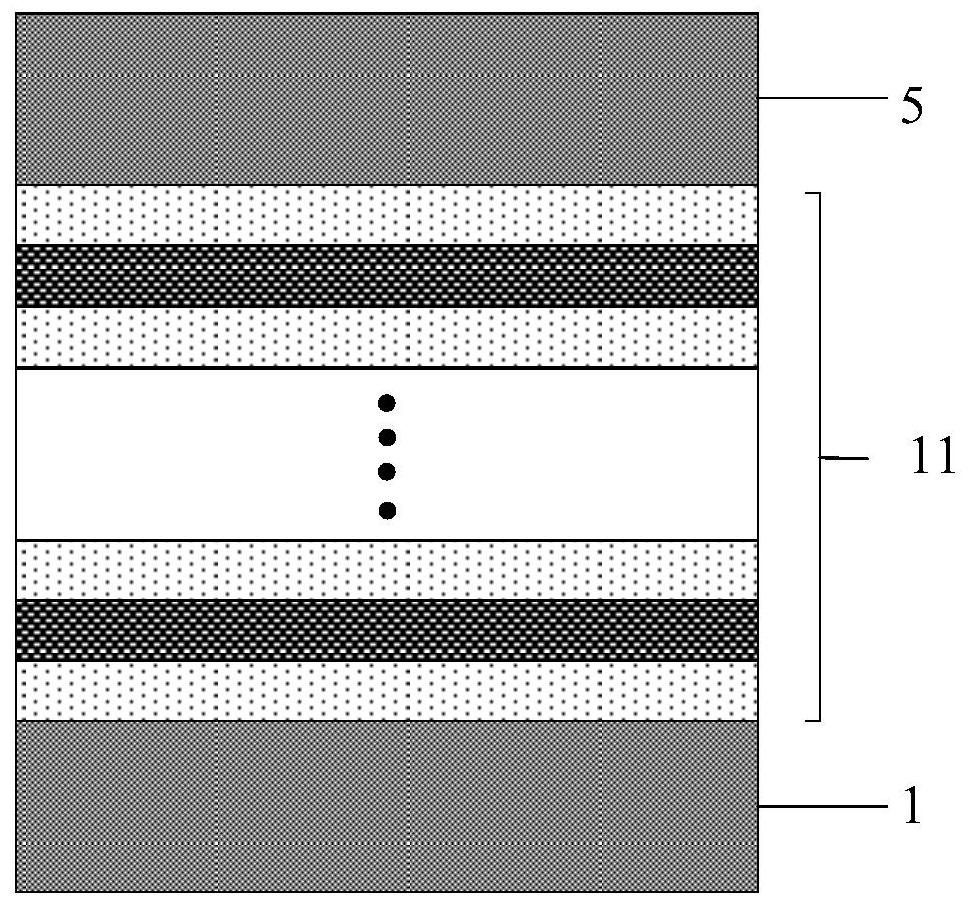
[0086] In the present invention, in step 1, N is an integer greater than or equal to 2, that is, there are at least two ferroelectric functional layers, and there is an insulating layer between two adjacent ferroelectric functional layers, that is, N ferroelectric functional layers Layers and N-1 insulating layers are alternately stacked to form an a...
Embodiment 1
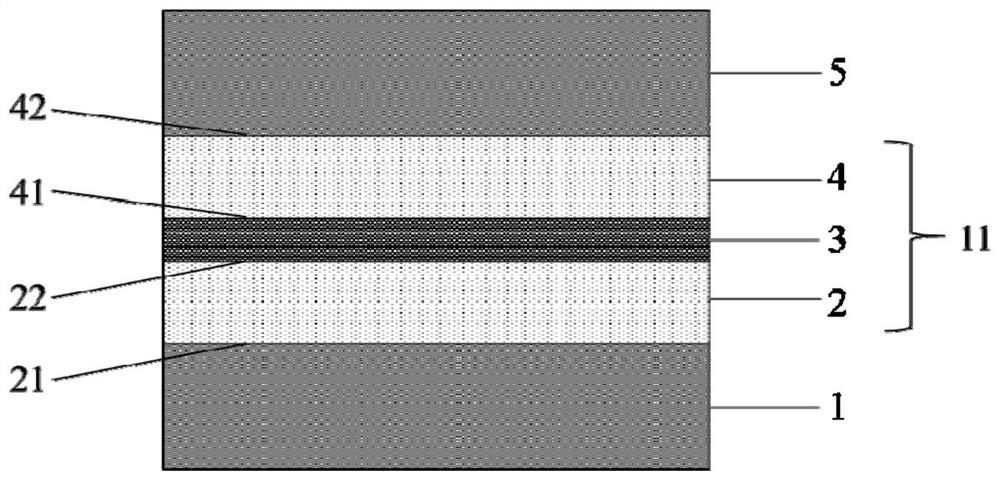
[0142] This embodiment provides a Hf-based 0.5 Zr 0.5 O 2 (hereinafter abbreviated as HZO) ferroelectric thin films and Al 2 O 3 The multi-value memory cell of the asymmetric ferroelectric tunnel junction of the insulating layer, its structure diagram is as follows figure 1 As shown, from bottom to top, it mainly includes a first electrode layer 1 , a first ferroelectric functional layer 2 , an insulating layer 3 , a second ferroelectric functional layer 4 , and a second electrode layer 5 . Specific steps are as follows:
[0143] (1) Preparation of the first electrode layer 1
[0144] Step 1: Prepare the first electrode layer 1: In the embodiment, TiN is used as the lower electrode 1, and SiO is polished and grown on one side by magnetron sputtering 2 A layer of lower electrode 1 is grown on the single crystal silicon substrate.
[0145] Step 1-1: Substrate cleaning: first use acetone to clean under ultrasonic environment for 10 minutes, then use alcohol to clean under ...
Embodiment 2
[0167] This embodiment provides a Si:HfO-based 2 and Al:HfO 2 Ferroelectric thin films and Al 2 O 3 The multi-value memory cell of the asymmetric ferroelectric tunnel junction of the insulating layer, its structure diagram is as follows figure 1 As shown, from bottom to top, it mainly includes a lower electrode 1 , a first ferroelectric functional layer 2 , an insulating layer 3 , a second ferroelectric functional layer 4 , and an upper electrode 5 . Specific steps are as follows:
[0168] (1) Preparation of the first electrode layer 1
[0169] Step 1: Prepare the first electrode layer 1: In the embodiment, TiN is used as the lower electrode 1, and SiO is polished and grown on one side by magnetron sputtering 2 A layer of lower electrode 1 is grown on the single crystal silicon substrate.
[0170] Step 1-1: Substrate cleaning: firstly use acetone to clean under ultrasonic environment for 10 minutes, then use alcohol to clean under ultrasonic environment for 10 minutes, r...
PUM
| Property | Measurement | Unit |
|---|---|---|
| thickness | aaaaa | aaaaa |
| thickness | aaaaa | aaaaa |
| thickness | aaaaa | aaaaa |
Abstract
Description
Claims
Application Information


