Substrate for micro LED display panel, and manufacturing method thereof

A display panel and manufacturing method technology, applied in the direction of instruments, electrical components, electrical solid devices, etc., can solve the problems of splicing screens such as large seams, falling off, and different thermal expansion coefficients, and achieve the effect of ensuring accuracy

Active Publication Date: 2020-06-02
BOE TECH GRP CO LTD +1
View PDF25 Cites 1 Cited by
  • Summary
  • Abstract
  • Description
  • Claims
  • Application Information

AI Technical Summary

Problems solved by technology

In an existing technology of super-large display through splicing, in order to achieve a very difficult seamless splicing, it is necessary to use glass front and back technology, and perform a through-hole process on the glass to realize the front and second surface circuit lines connection, but there are certain problems in the current method of metal plating in through holes, because in the subsequent process, the thermal expansion coefficients of metal and glass are different, causing the metal to easily expand and fall off from the hole in the subsequent high temperature process
In another prior art, the splicing method used is to use a flexible FPC to connect the upper and lower circuits. Although the connection can be realized, but because the thickness of the FPC is relatively large, the splicing seam caused by the splicing screen is extremely large, which affects the display. Effects and overall look

Method used


Image

  • Substrate for micro LED display panel, and manufacturing method thereof
  • Substrate for micro LED display panel, and manufacturing method thereof
  • Substrate for micro LED display panel, and manufacturing method thereof

Examples


Embodiment 1

[0063] Attached below Figure 2-9 Illustrate the manufacturing method of embodiment 1 of the present invention:

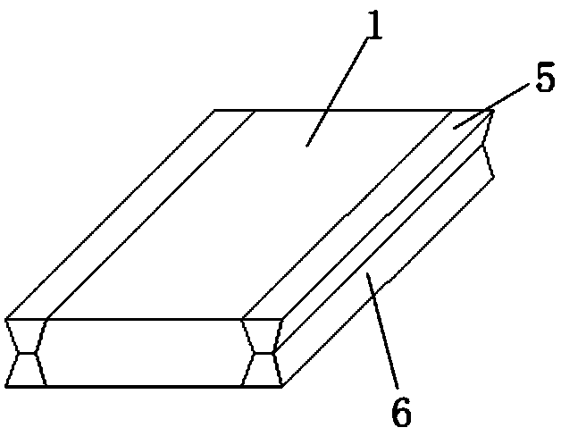
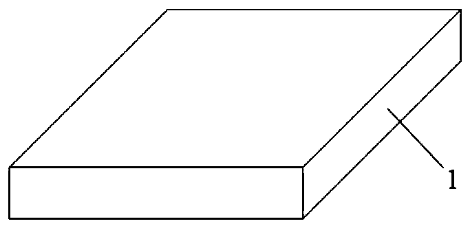
[0064] 1. Prepare the glass substrate ( figure 2 );

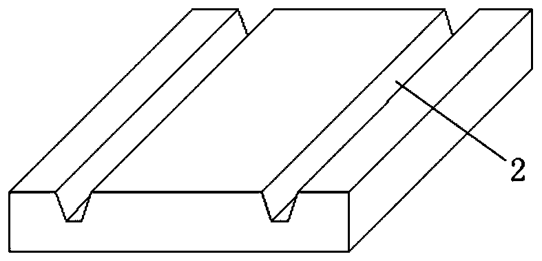
[0065] 2. Open the first strip-shaped hole 2 with a certain depth on the first surface of the glass substrate 1, the first strip-shaped hole 2, wherein the first strip-shaped hole 2 is two parallel at a certain distance ( image 3 );

[0066] 3. Form a metal layer 3 on the first surface of the glass substrate by vapor deposition, wherein the metal layer fills up the first strip-shaped hole 2 ( Figure 4 ).

[0067] 4. Form a photoresist 4 on the surface of the metal layer 3, and then expose and develop it (for example, using a mask plate), wherein the first part 41 of the photoresist corresponding to the first strip hole 2 remains, and other positions are photoresisted. Glue removal ( Figure 5 ).

[0068] 5. the substrate is etched, so that the metal layer at the first strip hole 2 position remains to f...


PUM


Abstract

The present application relates to a substrate for a micro LED display panel, and a manufacturing method thereof. The substrate comprises: a glass substrate; a first metal strip extending along the first side of the first surface of the glass substrate; and a second metal strip extending along the second side edge, corresponding to the first side edge, of the second surface of the glass substrate,wherein bottom surfaces of the first metal strip and the second metal strip are in contact with each other to make the first metal strip and the second metal strip form a structure for connecting partial metal of the first surface and the second surface of the glass substrate through metal on the side surface of the glass substrate. By the adoption of the substrate structure and the manufacturingmethod, the problem that when mobile printing is adopted at present, side edge circuits are prone to breakage and lack of glue is solved, the problem of large heat affected zone caused by laser cutting after copper deposition can be avoided, the difficulty of side edge gluing patterning is also avoided, metal cannot fall off, and the pattern precision is ensured.

Description

technical field [0001] The present application relates to the field of display technology, and in particular to the field of micro LED display in the field of display, and more specifically to a side metal structure and method for micro LED display. Background technique [0002] Micro-LED display panels have the characteristics of ultra-high pixel count, ultra-high resolution, low energy consumption, and long life. The technology is miniaturization and matrixing of micro-sized LED arrays. Compared with OLED, the distance between pixels can be reduced from mm to um, and the color gamut is high. The existing technology uses micro-transfer printing to make micro-LED arrays, and the light-emitting diode bare chips are separated from the sapphire substrate by laser lift-off technology. After opening, use a patterned transfer substrate to absorb the bare LED chip from the supply substrate and transfer it to the receiving substrate. This receiving substrate is a silicon substrate t...

Claims


Application Information

Patent Timeline
Patent Type & Authority Applications(China)
IPC IPC(8): G09F9/33
CPCG09F9/33H01L27/124H01L25/167H01L25/0753H01L33/62H01L27/1266H01L27/1288
Inventor 齐永莲杨虹曲连杰张珊赵合彬邱云
Owner BOE TECH GRP CO LTD
Why Eureka
Try Eureka