MEMS device and method of forming MEMS device

A dielectric layer and backplane technology, applied in the field of micro-electromechanical, can solve the problems of poor tensile properties of the backplane, the sensitivity and accuracy of the interference pull-in voltage test, etc., to ensure the tensile performance, facilitate the high sensitivity requirements, and improve the overall effect of stress

Active Publication Date: 2020-06-05
SEMICON MFG ELECTRONICS (SHAOXING) CORP +1
View PDF13 Cites 1 Cited by
  • Summary
  • Abstract
  • Description
  • Claims
  • Application Information

AI Technical Summary

Problems solved by technology

[0005] In the existing process, the backplane is usually composed of low-stress nitride and a low-stress conductive layer covering it. However, for other considerations (such as in order to improve the signal-to-noise rati

Method used


Image

  • MEMS device and method of forming MEMS device
  • MEMS device and method of forming MEMS device
  • MEMS device and method of forming MEMS device

Examples


Embodiment Construction

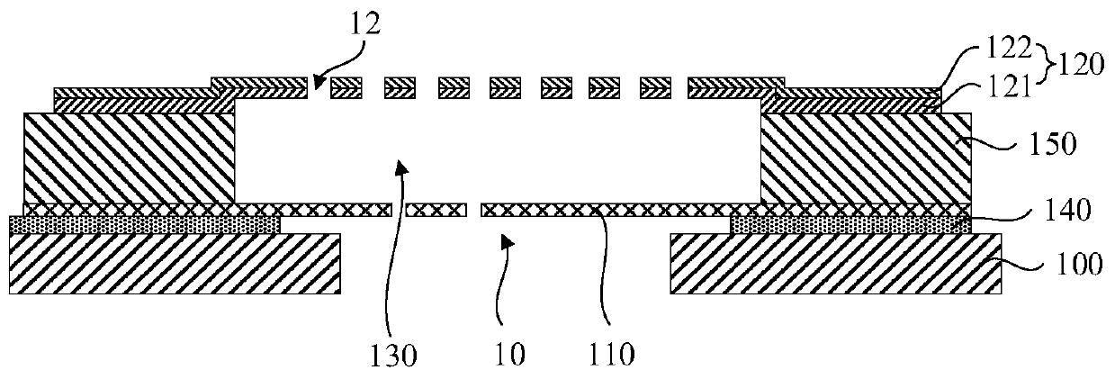
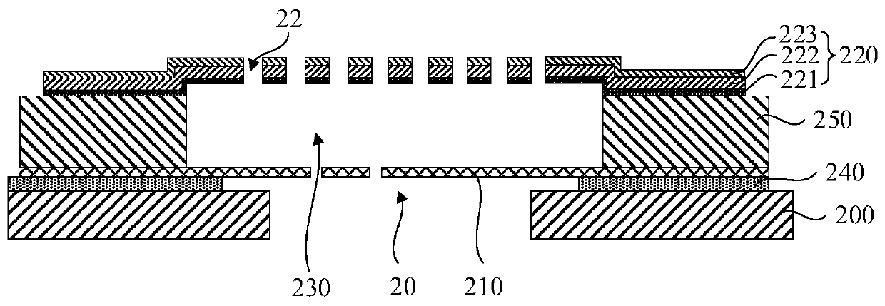
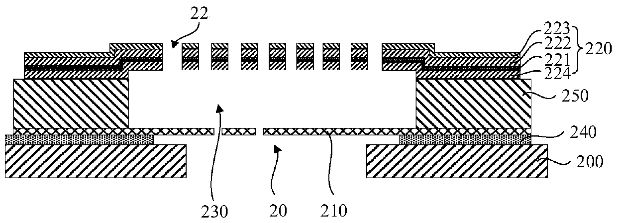
[0030] The MEMS device and the method for forming the MEMS device of the present invention will be further described in detail below with reference to the drawings and specific embodiments. The advantages and features of the present invention will become clearer from the following description. It should be noted that in the following description, many specific details and numerical values ​​are given in order to provide a more thorough understanding of the present invention. However, it is obvious to those skilled in the art that the present invention may not require one or more In other instances, some technical features known in the art are not described in order to avoid obscuring the present invention. It should be understood that the drawings in the description are all in very simplified form and use imprecise scales, and are only used to facilitate and clearly assist the purpose of illustrating the embodiments of the present invention.

[0031] For the convenience of de...


PUM

PropertyMeasurementUnit
Internal stressaaaaaaaaaa

Abstract

The invention relates to a MEMS device and a method of forming an MEMS device. In the MEMS device, a back plate comprises a first dielectric layer, a second dielectric layer and a conductive layer which are sequentially stacked. The stress level of the first dielectric layer is higher than that of the second dielectric layer, the overall stress and rigidity of the back plate can be improved by utilizing the first dielectric layer, the improvement of the sensitivity and accuracy of the test is facilitated when the pull-in voltage test is carried out, and the tensile property of the back plate is ensured while the larger size of the back plate is realized. In addition, since the conductive layer is still in contact with the second dielectric layer, the influence of the first dielectric layeron the contact performance of the conductive layer is small. In the MEMS device, a third dielectric layer can be arranged on the side, far away from the second dielectric layer, of the first dielectric layer so as to protect the first dielectric layer from being corroded. The method of forming an MEMS device can be used for forming the MEMS device.

Description

technical field [0001] The present invention relates to the field of micro-electromechanical technology, in particular to a MEMS device and a method for forming the MEMS device. Background technique [0002] Micro Electro Mechanical System (MEMS) integrates micro sensors, micro actuators, micro mechanical structures, micro power sources (micro energy sources), signal processing and control circuits, high-performance electronic integrated devices, interfaces, communications and other components. It can be regarded as an independent intelligent system, and its overall size is usually a few millimeters or even smaller. With the development trend of miniaturization of electronic devices, electronic devices including MEMS (hereinafter referred to as MEMS devices) such as MEMS microphones, MEMS accelerometers, MEMS gyroscopes, etc. have also made great progress and have broad development prospects. [0003] The manufacture of MEMS is different from traditional mechanical processi...

Claims


Application Information

Patent Timeline
IPC IPC(8): H04R19/00H04R31/00
CPCH04R19/005H04R31/00H04R31/003
Inventor 傅思宇陆晓龙刘国安
Owner SEMICON MFG ELECTRONICS (SHAOXING) CORP
Why Eureka
Try Eureka