Laser structures and methods for slot bonding of iii-v/silicon materials

A III-V, laser technology, used in lasers, laser parts, semiconductor lasers, etc., can solve the problems of inability to make light-emitting devices, unsuitable for integrated chip light source devices, etc., and achieve easy decomposition, reduce manufacturing processes, and simplify processes effect of steps

Active Publication Date: 2021-08-27
INST OF SEMICONDUCTORS - CHINESE ACAD OF SCI +1
View PDF7 Cites 0 Cited by
  • Summary
  • Abstract
  • Description
  • Claims
  • Application Information

AI Technical Summary

Problems solved by technology

However, as an indirect bandgap semiconductor, silicon materials cannot be used to make light-emitting devices, and are not suitable as light source devices in integrated chips.

Method used


Image

  • Laser structures and methods for slot bonding of iii-v/silicon materials
  • Laser structures and methods for slot bonding of iii-v/silicon materials
  • Laser structures and methods for slot bonding of iii-v/silicon materials

Examples


Embodiment Construction

[0050] In order to make the object, technical solution and advantages of the present invention clearer, the present invention will be further described in detail below in conjunction with specific embodiments and with reference to the accompanying drawings.

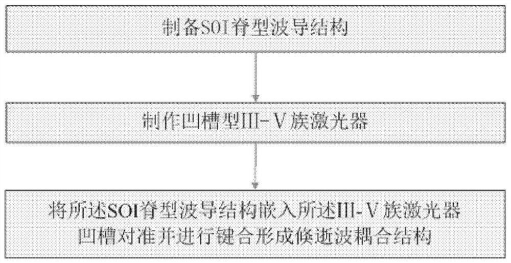
[0051] According to one embodiment of the present invention, there is provided a method for laser structure of III-V group / silicon material groove bonding, such as figure 1 Shown include:

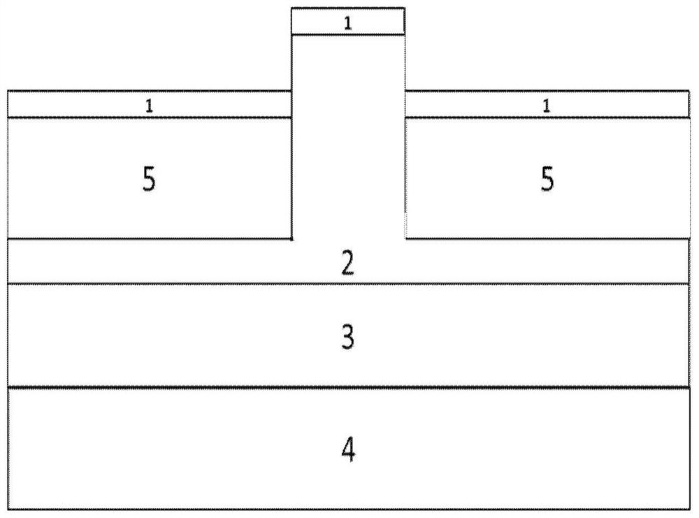
[0052] Step 1: preparing SOI ridge waveguide structure;

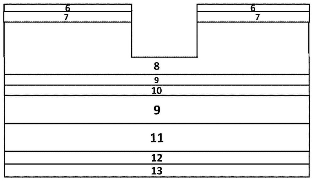
[0053] Step 2: Fabricate the groove type III-V group laser;

[0054] Step 3: Embedding the SOI ridge waveguide structure into the groove of the III-V laser for alignment and bonding. After bonding, an evanescent wave coupling structure is formed, and the laser light is coupled out from the SOI waveguide port.

[0055] Wherein, the order of step 1 and step 2 can be interchanged, that is, the order of preparing the ridge waveguide structure and manufacturing the III-V group lase...


PUM

PropertyMeasurementUnit
electrical resistanceaaaaaaaaaa
thicknessaaaaaaaaaa
thicknessaaaaaaaaaa

Abstract

The invention discloses a laser structure and method for slotting and bonding III-V group / silicon materials, and relates to the field of structural design of hybrid lasers. The method comprises: preparing a ridge waveguide structure; manufacturing a groove-type III-V group laser Embedding the ridge waveguide structure in the groove of the III-V laser for alignment and bonding, forming an evanescent wave coupling structure after bonding, and the laser light is coupled out from the SOI waveguide port. The invention adopts the groove structure laser and the silicon-based device to couple, and adopts the groove-type embedded structure in the longitudinal direction, which limits the offset distance of the silicon-based transmission device in space from the lateral direction, increases the bonding strength, and at the same time The difficulty of bonding is reduced; in addition, the present invention uses ZnO transparent conductive film to assist bonding hybrid laser, ZnO has good transmittance and can form a low-resistance conductive layer after a high-temperature film.

Description

technical field [0001] The invention relates to the field of structural design of hybrid lasers, in particular to a laser structure and a method for groove bonding of III-V groups and silicon materials. Background technique [0002] Fabrication of transmission devices on silicon-based wafers is the most mature and widely used basic material. The transmission structure formed by the refractive index difference between silicon and silicon oxide is suitable for light transmission in the communication band, and can well confine light in the transmission device. However, as an indirect bandgap semiconductor, silicon material cannot be used to make light-emitting devices, and is not suitable as a light source device in an integrated chip. The III-V semiconductor material is a direct bandgap semiconductor material, which can make a high-efficiency on-chip laser in the communication band. The hybrid laser combines the advantages of the two materials, but the two materials have dif...

Claims


Application Information

Patent Timeline
Patent Type & Authority Patents(China)
IPC IPC(8): H01S5/22H01S5/343
CPCH01S5/2202H01S5/343
Inventor 许兴胜秦璐靳思玥徐波
Owner INST OF SEMICONDUCTORS - CHINESE ACAD OF SCI
Why Eureka
Try Eureka