
Half-cut liquid crystal film and processing method

A processing method and technology of liquid crystal film, applied in nonlinear optics, instruments, optics, etc., can solve the problems of short circuit, electrical performance failure of liquid crystal film, easy short circuit and so on

Pending Publication Date: 2020-06-19
章思
View PDF7 Cites 1 Cited by
  • Summary
  • Abstract
  • Description
  • Claims
  • Application Information

AI Technical Summary

Problems solved by technology

When the ultraviolet laser is fully cut, the cutting part will cause the internal fracture of the material at the molecular level. Although it will not cause the upper and lower conductive layers to stick together and break the conduction, the cutting surface is not smooth enough, and the slag is serious, and the slag falls into the liquid crystal. When it is in the film and the shell, on the one hand, it will cause difficulties in subsequent assembly, and on the other hand, it will affect the writing of the finished product
CO 2 When the laser is fully cut, the liquid crystal film needs to be cut off, and the cutting energy required is relatively large. Although it can make the cut surface smooth without slag, it is very easy to cause the first conductive layer and the second conductive layer to stick together. Together, this leads to the failure of the electrical properties of the liquid crystal film - causing a short circuit problem, making the product's drive circuit board unable to power on the liquid crystal film normally and unable to complete the handwriting removal action
[0004] Therefore, for the technology, the required size of the liquid crystal film formed after full cutting either has the problem of conductive layer adhesion and easy short circuit, or has the problem of slag drop, so it needs to be further improved.

Method used


Image

  • Half-cut liquid crystal film and processing method
  • Half-cut liquid crystal film and processing method
  • Half-cut liquid crystal film and processing method

Examples


Embodiment 1

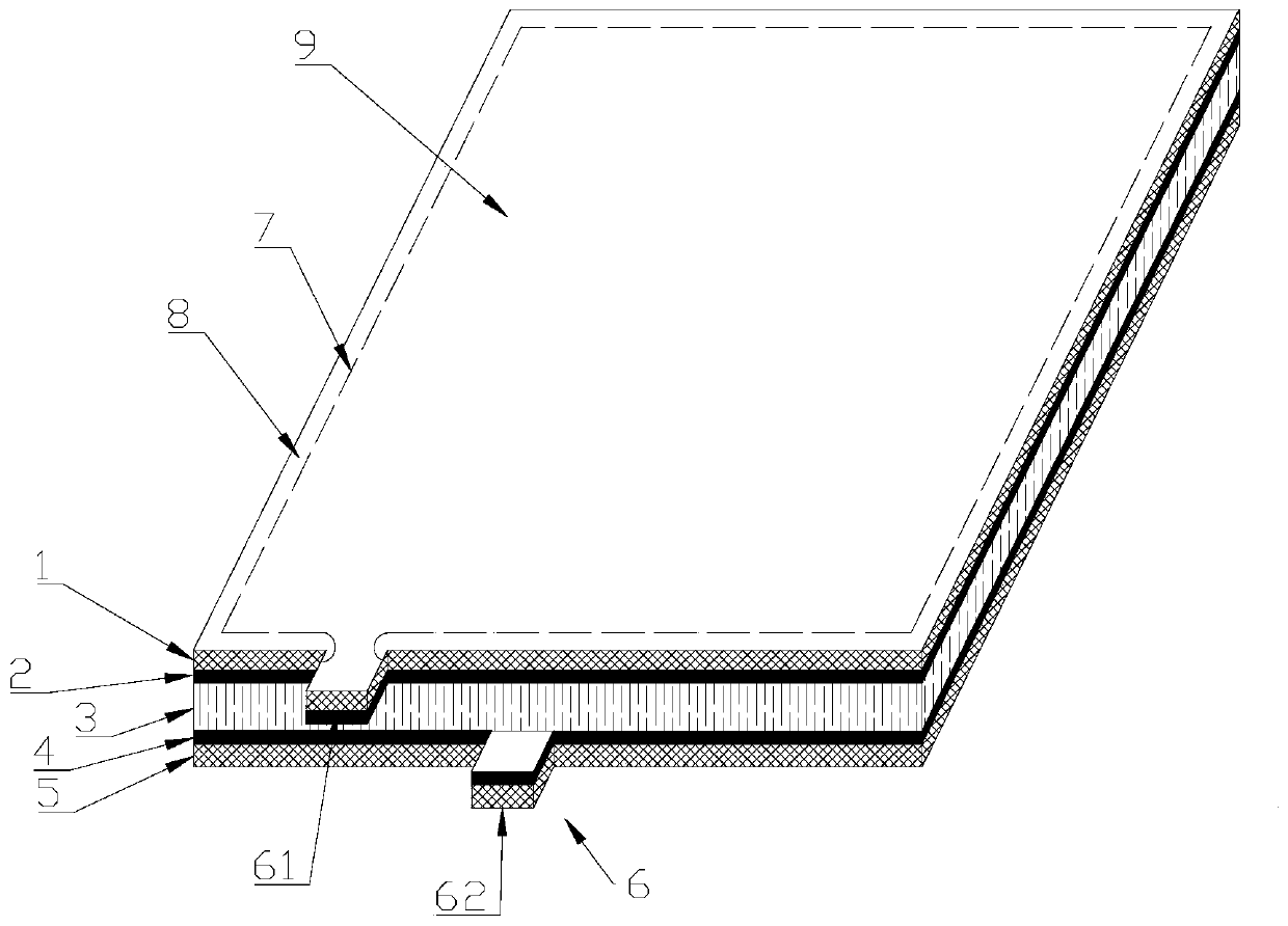
[0051] The half-cut line 7 penetrates vertically from the surface of the first substrate 1 toward the direction of the liquid crystal layer 3 , and its depth reaches at least the surface of the first conductive layer 2 facing away from the first substrate 1 . For example, the half-cut line 7 may go deep into the liquid crystal layer 3 , or the half-cut line 7 may go deep into the joint of the first conductive layer 2 and the liquid crystal layer 3 . In order to control the cutting depth conveniently, the half-cutting line 7 preferably goes deep into the liquid crystal layer 3 , so that it can guarantee cutting the first conductive layer 2 without cutting the second conductive layer 4 . For the convenience of description, in this embodiment, the half cut 7 goes deep into the liquid crystal layer 3 as an example for description. When the depth of the half-cut 7 is different, the same technical effect can be achieved by making adaptive modifications according to the content of t...

Embodiment 2

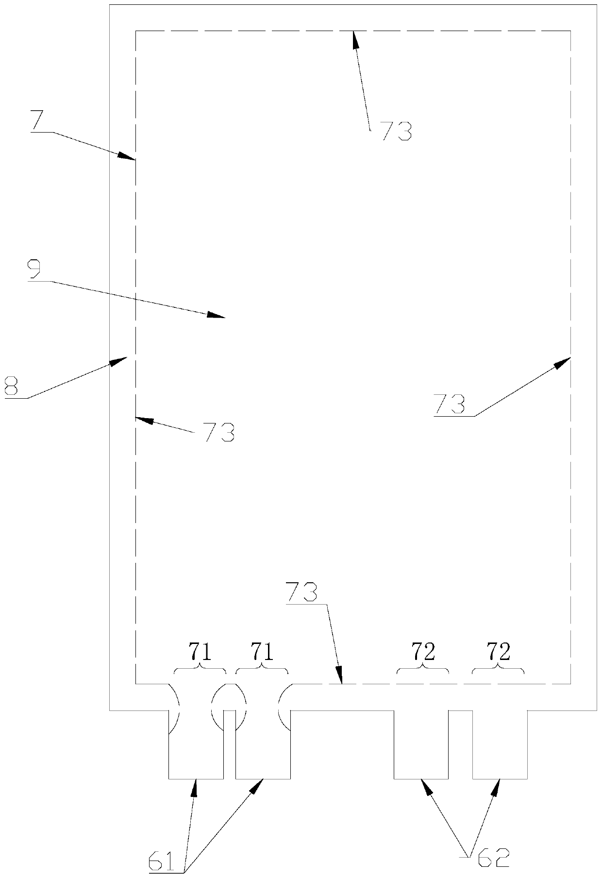
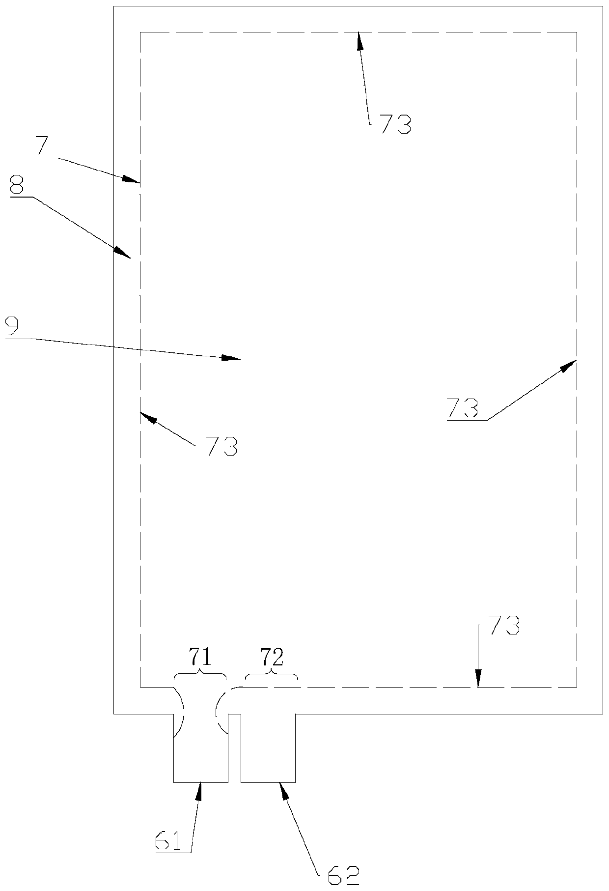
[0066] The half-cut line 7 penetrates vertically from the surface of the second substrate 5 toward the direction of the liquid crystal layer 3 , and its depth reaches at least the surface of the second conductive layer 4 facing away from the second substrate 5 . For example, the half-cut line 7 may go deep into the liquid crystal layer 3 , or the half-cut line 7 may go deep into the joint of the second conductive layer 4 and the liquid crystal layer 3 . In order to control the cutting depth conveniently, the half-cutting line 7 preferably goes deep into the liquid crystal layer 3 , so that it can guarantee cutting the second conductive layer 4 without cutting the first conductive layer 2 .

[0067] Such as Figure 4 , Figure 5 As shown, the half cut line 7 divides the liquid crystal film into an outer ring portion 8 and an inner ring portion 9 . Among them, what is located inside the half-cut line 7 is the inner ring portion 9 , and what is located outside the half-cut lin...

Embodiment 3

[0081] The half-cutting line 7 penetrates vertically from the surface of the first substrate 1 or the second substrate 5 to the direction of the liquid crystal layer 3, and its deep depth needs to ensure that at least one conductive layer is cut, and that the entire liquid crystal film does not was cut off. For example, the half-cut line 7 can go deep into the liquid crystal layer 3, or the half-cut line 7 can go deep into the joint position of the second conductive layer 4 and the liquid crystal layer 3, or the half-cut line 7 can go deep into the liquid crystal layer 3. The part where the liquid crystal layer 3 is combined with the first conductive layer 2, or the half-cut line 7 can go deep into the second substrate 5 from the direction of the first substrate 1 without cutting the second substrate 5, or the half-cut line 7 can be formed by The direction of the second substrate 5 penetrates into the first substrate 1 without cutting the first substrate 1 .

[0082] Such as ...


PUM


Abstract

The invention relates to a half-cut liquid crystal film and a processing method, the half-cut liquid crystal film comprises a first substrate, a first conductive layer, a liquid crystal layer, a second conductive layer and a second substrate, and the half-cut liquid crystal film is characterized in that a half-cut line formed by half cutting is arranged at a preset distance in the edge of the liquid crystal film, and the half-cut line at least penetrates into one of the first conductive layer and the second conductive layer. According to the invention, through half-cutting, the two internal conductive layers are not conducted; accordingly, during full cutting, even if the conductive layer in the outermost edge is adhered, the electrical property of the whole liquid crystal film cannot be invalid; thus, in the machining process, during full cutting, a smooth outer tangent plane without slag falling can be obtained by utilizing the cutting advantage of the CO2 laser; during half-cutting,the electrical performance failure of the liquid crystal film can be avoided by utilizing the advantages of ultraviolet cutting, so that all the advantages of ultraviolet cutting and CO2 laser cutting in the prior art can be combined, the defects of ultraviolet cutting and CO2 laser cutting can be eliminated, and a required product can be obtained.

Description

【Technical field】 [0001] The invention relates to a liquid crystal film, in particular to a half-cut liquid crystal film and a processing method. 【Background technique】 [0002] With the development of the information society, the application of liquid crystal writing devices is becoming more and more common. At present, the industry of liquid crystal writing devices has begun to form in China and is developing at a high speed. In the prior art, a liquid crystal writing device usually includes a driving circuit board and a liquid crystal film, and the liquid crystal film includes a first substrate, a first conductive layer, a liquid crystal layer, a second conductive layer and a second substrate. The first conductive layer and the second conductive layer are usually formed by attaching conductive substances such as ITO to the first substrate and the second substrate. The liquid crystal layer is located between the first conductive layer and the second conductive layer, which...

Claims


Application Information

Patent Timeline
Patent Type & Authority Applications(China)
IPC IPC(8): G02F1/1333G02F1/1343G02F1/133
CPCG02F1/133351G02F1/1343G02F1/133
Inventor 章思
Owner 章思
Learn More