Array substrate, manufacturing method thereof and display device

A technology of an array substrate and a manufacturing method, which is applied in the field of display, and can solve problems such as prone to sharp edges, poor coverage, poor short-circuiting of gate lines and data lines, etc.

Active Publication Date: 2020-06-19
HEFEI XINSHENG OPTOELECTRONICS TECH CO LTD +1
View PDF4 Cites 0 Cited by
  • Summary
  • Abstract
  • Description
  • Claims
  • Application Information

AI Technical Summary

Problems solved by technology

Wrinkles will appear at the same position during the process of forming the source and drain metal layer (SD). SD is thinner and prone to sharp edges in the wrinkled area due to poor coverage.
If an electrostatic effect or an

Method used


Image

  • Array substrate, manufacturing method thereof and display device
  • Array substrate, manufacturing method thereof and display device
  • Array substrate, manufacturing method thereof and display device

Examples


Embodiment Construction

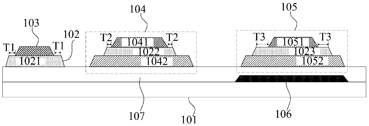
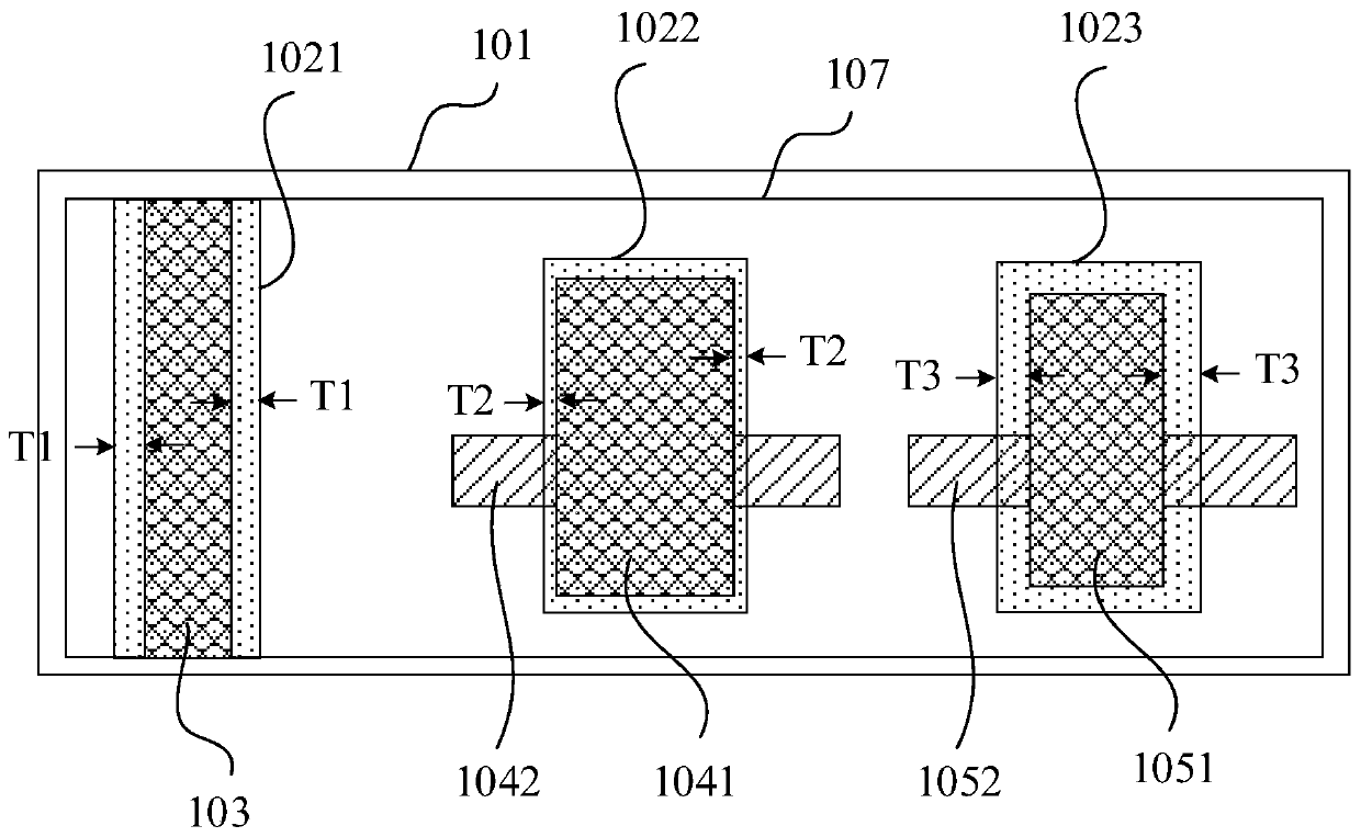
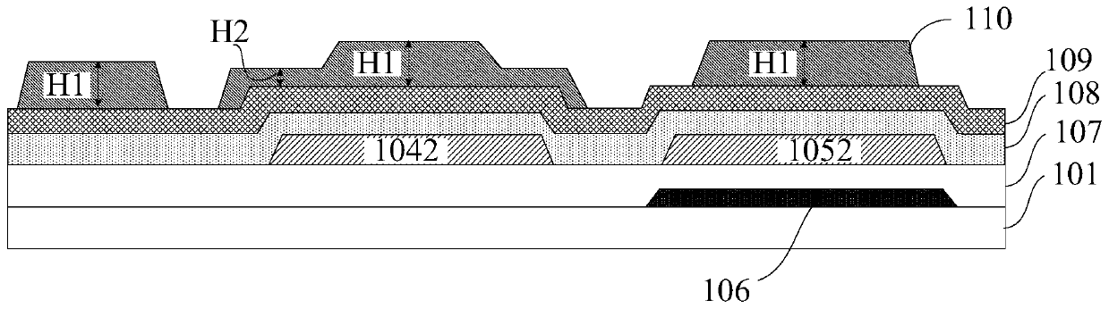
[0043] In order to make the purpose, technical solutions and advantages of the embodiments of the present invention more clear, the following will clearly and completely describe the technical solutions of the embodiments of the present invention in conjunction with the drawings of the embodiments of the present invention. The thickness and shape of each film layer in the drawings do not reflect the real scale, and the purpose is only to illustrate the content of the present invention. Apparently, the described embodiments are some, not all, embodiments of the present invention. Based on the described embodiments of the present invention, all other embodiments obtained by persons of ordinary skill in the art without creative efforts shall fall within the protection scope of the present invention.

[0044] Unless otherwise defined, the technical terms or scientific terms used herein shall have the usual meanings understood by those skilled in the art to which the present invent...


PUM


Abstract

The invention discloses an array substrate, a manufacturing method thereof and a display device. The array substrate comprises a gate insulating layer, a gate line and a switching transistor which arelocated on a substrate, the gate insulating layer comprises a first part covering the gate line and a second part covering a gate of the switching transistor; a first distance is formed between an edge of the first part and an edge of the gate line; the first distance is greater than a second distance between an edge of the second part and a gate edge of the switching transistor; equivalently, the GI tail of the gate insulating layer in a switching transistor region is not changed; the GI tail in a gate line region is increased; a subsequent interlayer dielectric layer continuously completestwo climbing processes; due to the fact that the distance between an edge of the gate insulating layer and the edge of the gate line is large, the interlayer dielectric layer is not prone to wrinkles,a subsequent source-drain metal layer cannot be thinned or sharp due to the wrinkles, the DGS defect can be well overcome, meanwhile, the structure of the switching transistor is not changed, it is guaranteed that no newly-added defect exists, and the product yield is increased.

Description

technical field [0001] The present invention relates to the field of display technology, in particular to an array substrate, a manufacturing method thereof and a display device. Background technique [0002] At present, active matrix electroluminescent display products (AMOLED) are moving towards high definition, large size and high refresh rate. This puts a higher requirement on the performance of the transistor (TFT) of the AMOLED driving circuit. Currently, the TFT structures used in AMOLED driving circuits mainly include etch stop layer structure (ESL), top gate structure (Top Gate), and back channel etch structure (BCE). Among them, there is no overlap between the gate and the source and drain of the Top Gate structure, so it can effectively reduce the parasitic capacitance, and the refresh frequency is better, the size is smaller, and it can better meet the needs of AMOLED development. Therefore, the Top Gate structure is a focus of research and development. directi...

Claims


Application Information

Patent Timeline
IPC IPC(8): H01L27/12H01L21/77H01L27/32
CPCH01L27/1214H01L27/1237H01L27/1259H10K59/12
Inventor 胡迎宾赵策丁远奎王庆贺刘宁宋嘉文宋威闫梁臣
Owner HEFEI XINSHENG OPTOELECTRONICS TECH CO LTD
Why Eureka
Try Eureka