Diode packaging method
A packaging method and diode technology, applied in the direction of electrical components, circuits, semiconductor devices, etc., can solve the problems of reduced production efficiency of diodes, uneven baking temperature, long baking time, etc., to avoid glue cracking, ensure hardening effect, Improves the effect of baking
- Summary
- Abstract
- Description
- Claims
- Application Information
AI Technical Summary
Problems solved by technology
Method used
Image
Examples
Embodiment Construction
[0029]In order to make the technical means, creative features, goals and effects achieved by the present invention easy to understand, the present invention will be further described below in conjunction with specific embodiments.
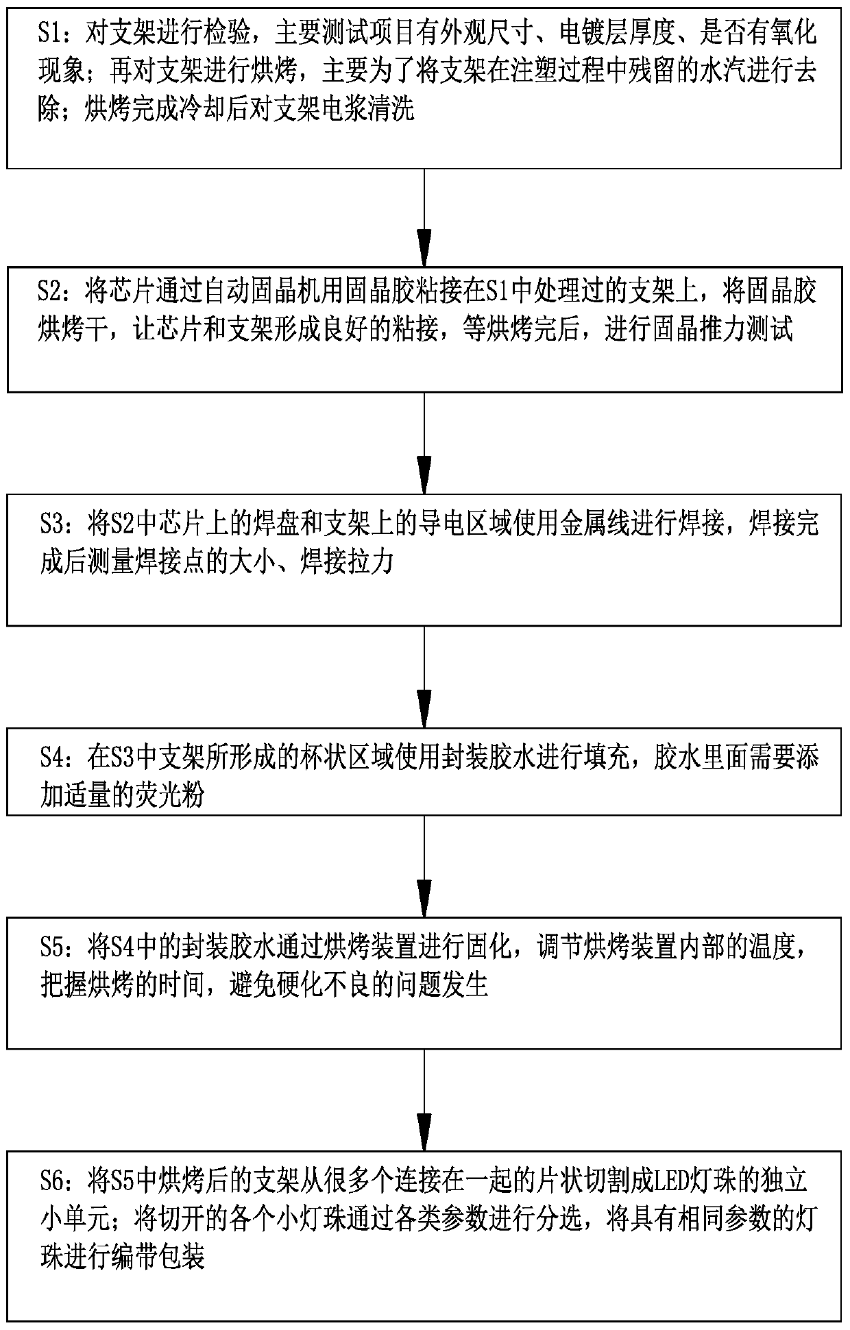
[0030] Such as Figure 1 to Figure 6 Shown, a kind of diode packaging method described in the present invention comprises the following steps:
[0031] S1: Inspect the bracket, the main test items are the appearance size, the thickness of the electroplating layer, and whether there is oxidation; then bake the bracket, mainly to remove the residual water vapor in the injection molding process of the bracket; Bracket plasma cleaning, plasma cleaning is mainly to form an arc with hydrogen and oxygen inside the equipment to remove residual organic matter on the surface of the bracket and improve the bonding force of the solid crystal;
[0032] S2: Bond the chip on the bracket treated in S1 with a die-bonding adhesive through an automatic die-bonding m...
PUM
 Abstract
Description
Claims
Application Information


