Manufacturing method of multilayer local thick copper circuit board

A local thick copper and manufacturing method technology, which is applied in multilayer circuit manufacturing, printed circuit manufacturing, printed circuit, etc., can solve the problems of large difference in thermal expansion coefficient between copper block and PCB, easy delamination and explosion, cumbersome production process, etc. , to avoid cracking and board warping, eliminate the risk of difficult production, and high difficulty in operation

Inactive Publication Date: 2020-06-19
KINWONG ELECTRONICS TECH LONGCHUAN
View PDF6 Cites 4 Cited by
  • Summary
  • Abstract
  • Description
  • Claims
  • Application Information

AI Technical Summary

Problems solved by technology

[0003] Such as the patent document whose publication number is CN10533875A, it discloses a kind of production of local thick copper by the positive process mode of copper plating of the first circuit and thickening of local copper plating for the second time, which realizes local thick copper plating well, but this method is easy Problems such as sandwich film, uneven copper thickness, and multiple electroplating are required
[0004] For example, the patent document with the publication number CN108282967A discloses that the local thick copper is made by SMT welding, and the thick copper strip punched out according to the local thick copper requirements is welded on the position where the PCB needs to be thickened by SMT, which is well realized. A thick copper area with a large difference in thickness has been realized, but the production process of this invention is cumbersome and the processing quality is not guaranteed; there are restrictions on the difference in copper thickness, the size of local thick copper and the number of local thick copper
[0005] For example, the patent document with the publication number CN109475051A discloses a method of making local thick copper by embedding copper blocks. This process is relatively simple and easy to implement, but it requires the copper thickness of the local thick copper to be greater than or equal to 0.8mm, which has great limitations. , and it is easy to cause cracking and board warping, and the thermal expansion coefficient of copper block and PCB is quite different. After reflow soldering and thermal stress test, it is easy to delaminate and explode, and it is not easy to achieve mass production.

Method used


Image

  • Manufacturing method of multilayer local thick copper circuit board
  • Manufacturing method of multilayer local thick copper circuit board
  • Manufacturing method of multilayer local thick copper circuit board

Examples


Embodiment Construction

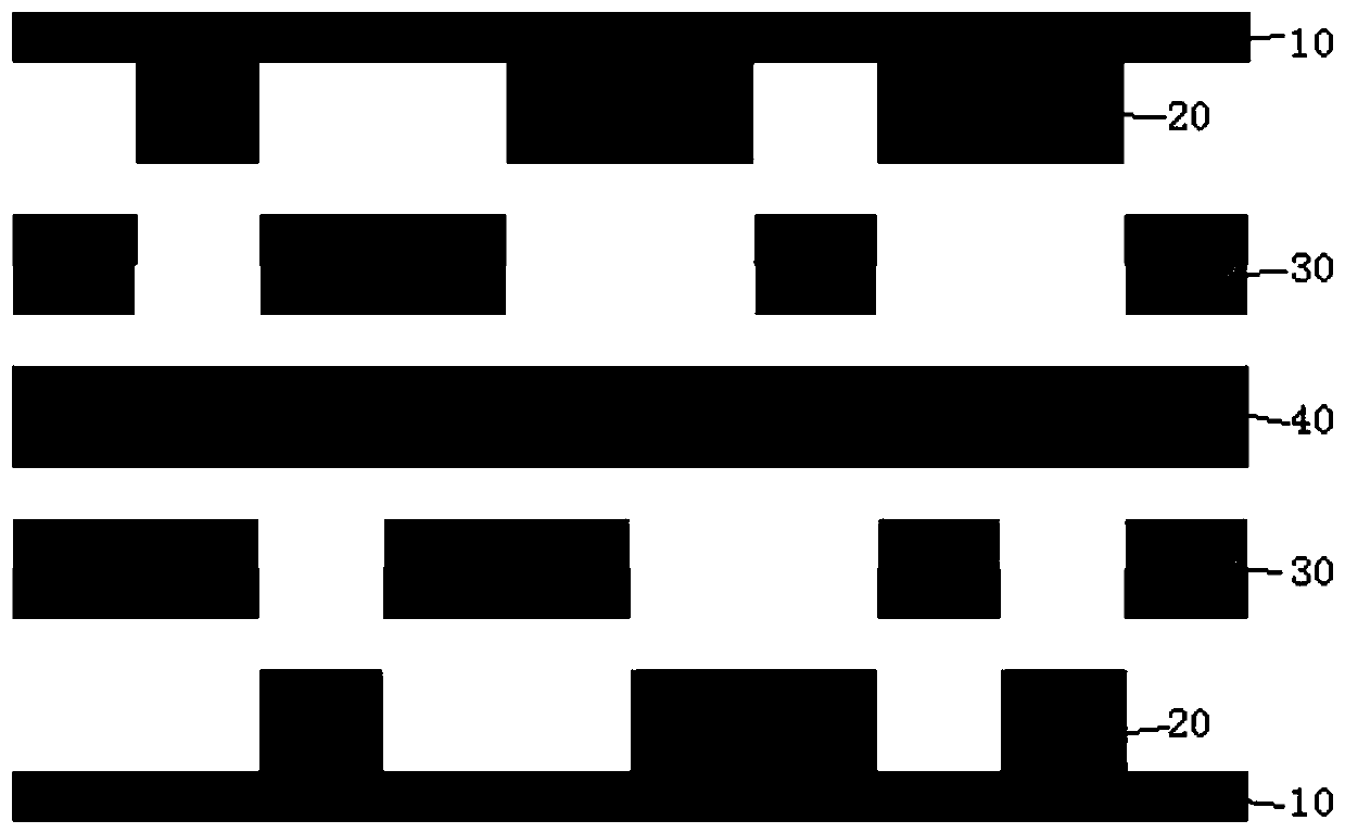
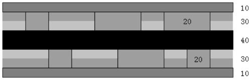
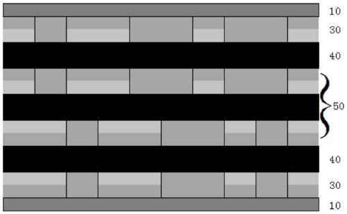
[0033] The technical solutions in the embodiments of the present invention will be clearly and completely described below in conjunction with the drawings in the embodiments of the present invention, and similar component numbers in the drawings represent similar components. Apparently, the embodiments described below are only a part of the embodiments of the present invention, rather than all the embodiments. Based on the embodiments of the present invention, all other embodiments obtained by persons of ordinary skill in the art without creative efforts fall within the protection scope of the present invention.

[0034] It should be understood that when used in this specification and the appended claims, the terms "comprising" and "comprises" indicate the presence of described features, integers, steps, operations, elements and / or components, but do not exclude one or Presence or addition of multiple other features, integers, steps, operations, elements, components and / or col...


PUM

PropertyMeasurementUnit
thicknessaaaaaaaaaa
thicknessaaaaaaaaaa
thicknessaaaaaaaaaa

Abstract

The invention discloses a manufacturing method of a multilayer local thick copper circuit board, and relates to the technical field of circuit board manufacturing. The method comprises the steps: S1,attaching thick copper foil to a carrier plate, and the thickness of the thick copper foil being the same as the preset local copper thickness; S2, the thick copper foil being provided with a thick copper area and a non-thick copper area, and removing the non-thick copper area of the thick copper foil through laser cutting; S3, performing windowing on the core plate, the windowing area being the same as the thick copper area, and the windowing size being 0.05-0.2 mm larger than the size of the thick copper area; and S4, carrying out browning treatment on the thick copper foil and the core plate obtained in the step S2, and carrying out press fit according to the structure of a carrier plate, the thick copper foil, the core plate, a prepreg, the core plate, the thick copper foil and the carrier plate to obtain the multilayer plate with local thick copper. Aiming at the circuit board with the local copper thickness of 3-10oz, the whole thick copper foil is embedded, and the circuit boardwith the local thick copper is manufactured by cutting the local thick copper area on the thick copper foil, so that the process is simplified, and the cost is saved.

Description

technical field [0001] The invention relates to the technical field of circuit board production, in particular to a method for manufacturing a multilayer local thick copper circuit board. Background technique [0002] With the rapid development of electronic products in the direction of thinning, miniaturization and high integration, higher requirements are put forward for the stability of high-current operation, high-voltage resistance, safety, durability and high thermal conductivity of printed circuit boards. requirements. In order to make the PCB board meet the requirements of heat dissipation and high current at the same time, the method of increasing the copper thickness of the PCB conductor, local thick copper, and embedding copper wires and copper blocks in the multilayer board is usually used. Locally thick copper can be produced in a variety of techniques, but there are still some problems, including: [0003] Such as the patent document whose publication number ...

Claims


Application Information

Patent Timeline
Patent Type & Authority Applications(China)
IPC IPC(8): H05K3/46H05K3/02
CPCH05K3/027H05K3/4611
Inventor 李少强殷景锋林友锟
Owner KINWONG ELECTRONICS TECH LONGCHUAN
Why Eureka
Try Eureka