Method for realizing ultra-fine package lead based on photolithography and electroplating

A packaging lead, ultra-fine technology, applied in the direction of circuits, electrical components, electric solid devices, etc., can solve the problems of insufficient lead structure strength, complex capillary design, limited strength of copper materials, etc., achieve good planarization effect and overcome structural strength Insufficient, Effect of High Coating Thickness Uniformity

Active Publication Date: 2018-07-03
SHANGHAI JIAO TONG UNIV
View PDF3 Cites 1 Cited by
  • Summary
  • Abstract
  • Description
  • Claims
  • Application Information

AI Technical Summary

Problems solved by technology

These will make the capillary design more complicated and difficult to realize
At the same time, the copper material itself has limited strength. When the wire diameter is significantly reduced, there is a problem of insufficient lead structure strength.

Method used


Image

  • Method for realizing ultra-fine package lead based on photolithography and electroplating
  • Method for realizing ultra-fine package lead based on photolithography and electroplating

Examples


Embodiment 1

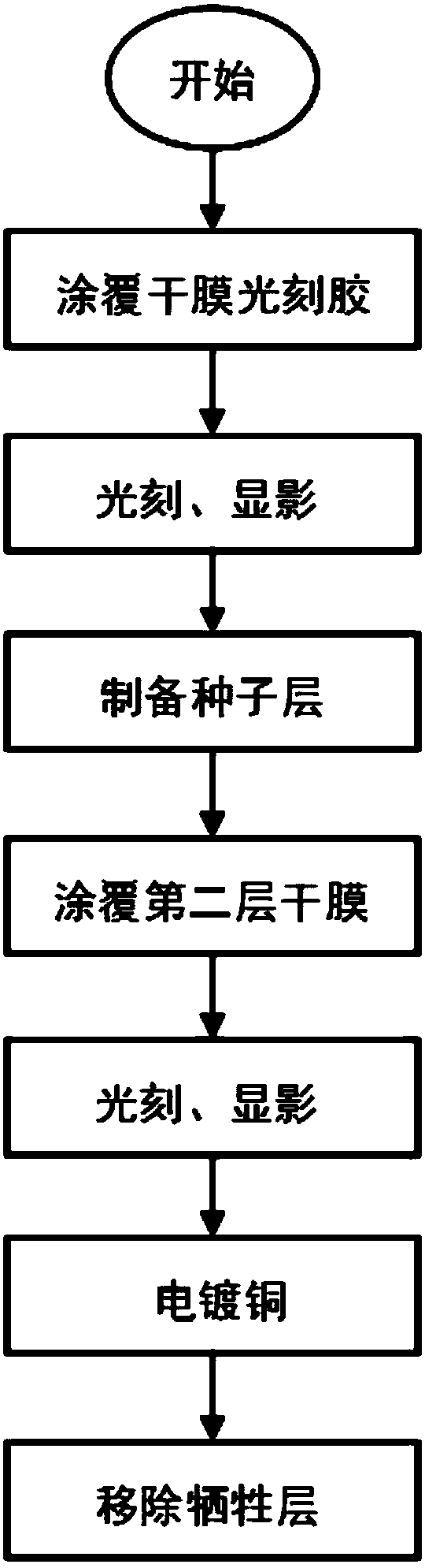
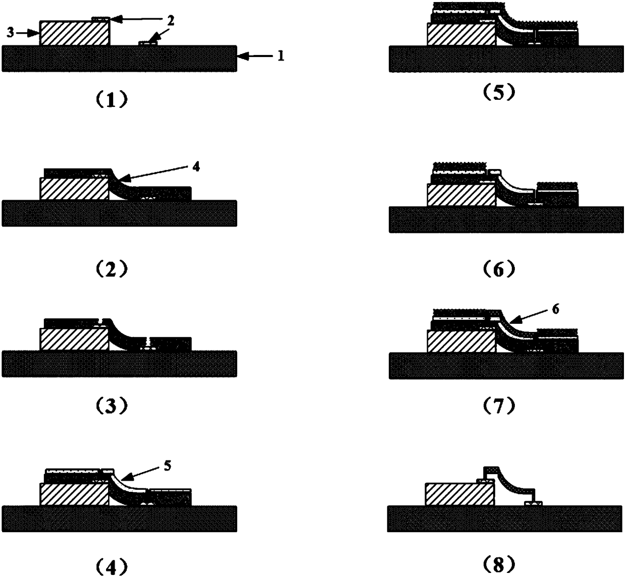
[0046] This embodiment provides a method for realizing ultra-fine packaging leads based on photolithography and electroplating, which uses photolithography and electroplating instead of wire bonding to realize the connection between electrodes.

[0047] Described method specifically comprises the steps:

[0048] 1) Coating a layer of 20 μm thick dry film photoresist on the surface of the glass substrate fixed with a 20 μm thick chip and a metal pad;

[0049] In this step, the substrate can be made of glass, and the dry film photoresist can be coated with hot rolling technology; of course, in other embodiments, the thickness of the chip and the thickness of the dry film can be adjusted according to the actual situation.

[0050] 2) Expose and develop the substrate processed in step 1), develop a group of via holes with a size of 20 μm on the metal pads of the chip and the substrate respectively, and use the two via holes facing the chip and the substrate The holes are a group,...

Embodiment 2

[0061] This embodiment provides a method for realizing ultra-fine packaging leads based on photolithography and electroplating, which uses photolithography and electroplating instead of wire bonding to realize the connection between electrodes.

[0062] Described method specifically comprises the steps:

[0063] 1) Coating a layer of 60 μm thick dry film photoresist on the surface of the silicon wafer substrate fixed with a 100 μm thick chip and a metal pad;

[0064] In this step, the substrate can be a silicon wafer, and the dry film photoresist can be coated with a vacuum lamination technique; of course, in other embodiments, the thickness of the chip and the thickness of the dry film can be adjusted according to actual conditions.

[0065] 2) Expose and develop the substrate processed in step 1), and develop via holes with a size of 50 μm on the metal pads of the chip and the substrate respectively, taking the two via holes facing each other on the chip and the substrate as...


PUM

PropertyMeasurementUnit
thicknessaaaaaaaaaa
thicknessaaaaaaaaaa
widthaaaaaaaaaa

Abstract

The invention discloses a method for realizing ultra-fine package lead based on photolithography and electroplating. The method comprises a step of coating a surface of a substrate with the fixation of a chip and metal pads with a layer of dry film photoresist, a step of carrying out photolithography and development and showing through holes in a dry film on the chip and the metal pads, a step ofpreparing a seed layer on a formed surface, a step of coating the surface of the seed layer with a layer of dry film photoresist, a step of carrying out photolithography and development again such that the through holes on the metal pads and the seed layer under a lead between the through holes are exposed, a step of plating the surface of the exposed seed layer with a layer of copper and forminga lead between the metal pads, and a step of removing the dry film photoresist and the seed layer as sacrificial layers and finally forming a floating lead interconnect structure. According to the method, wire bonding is replaced by the photolithography and electroplating process, the connection between the chip and the substrate pads is achieved, the size of the lead is not restricted by a traditional wire bonding process, and so the feature size of the lead can be further reduced to the precision of photolithography.

Description

technical field [0001] The invention relates to the field of microelectronic packaging, in particular to a method for realizing ultra-fine packaging leads based on photolithography and electroplating. Background technique [0002] With the rapid development of the microelectronics industry, the integration of integrated circuit chips has increased, and finer leads and higher numbers of input / output ports have become an inevitable development trend. Currently, the most common interconnect technology is wire bonding, especially ball bonding. When packaging, wire bonding is required on finer pads, and small packages require ultra-fine wire bonding, and the pad pitch must be reduced accordingly. In addition, the need to reduce manufacturing costs and improve performance is also driving the device's ultra-fine pitch and high-density, multiple input / output port packaging. [0003] The main advantages of fine and ultra-fine pitch wire bonding are increased input / output port count...

Claims


Application Information

Patent Timeline
Patent Type & Authority Applications(China)
IPC IPC(8): H01L23/49H01L21/48
CPCH01L21/4814H01L21/4846H01L21/4885H01L23/49H01L2224/82001H01L2224/18
Inventor 戴旭涵李冬洋丁桂甫姜太圭
Owner SHANGHAI JIAO TONG UNIV
Why Eureka
Try Eureka