Semiconductor phosphor

A semiconductor and phosphor technology, applied in the field of semiconductor phosphors, can solve problems such as insufficient luminous efficiency, and achieve stable efficiency, easy adjustment, and high efficiency

Pending Publication Date: 2020-06-19
SHIN-ETSU HANDOTAI CO LTD
View PDF4 Cites 0 Cited by
  • Summary
  • Abstract
  • Description
  • Claims
  • Application Information

AI Technical Summary

Problems solved by technology

However, since the light receiving part and the light emitting part are separated from each other, the luminous efficiency is not sufficient

Method used


Image

  • Semiconductor phosphor
  • Semiconductor phosphor
  • Semiconductor phosphor

Examples


Embodiment 1

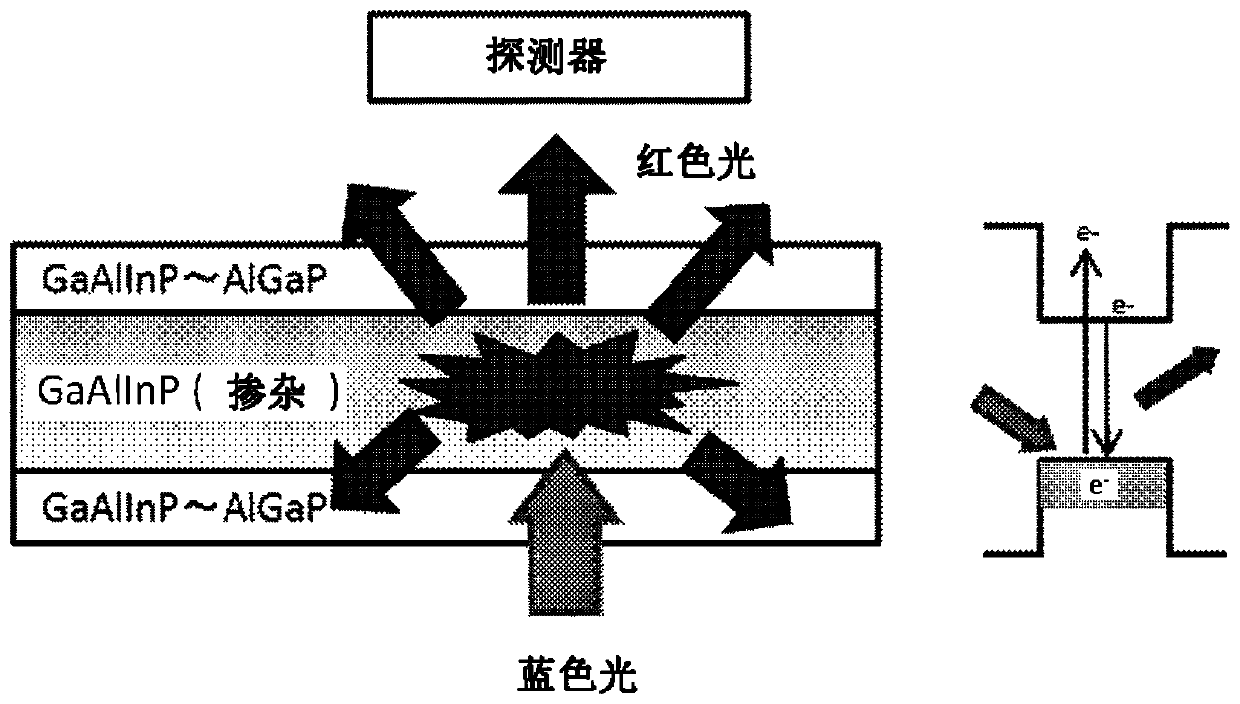
[0070] Using the red area as the target, use the MOVPE device to make Figure 14 The shown AlGaInP multilayer films were grown on GaAs substrates. The layer responsible for PL light emission is set to MQW of GaInP (well layer) / AlInP (barrier layer), and the target wavelength is set to a peak wavelength of 635 [nm]. Set the dopant as Si and the carrier concentration as 3.5E17[ / cm 3 ]. Thereafter, the GaAs substrate is removed by chemical etching in order to absorb wavelengths near the target wavelength, and then the grown multilayer thin film is bonded to the sapphire substrate with an adhesive to produce a semiconductor-type phosphor. The obtained semiconductor-type phosphor has a multi-quantum well structure with forty sets of active layers and barrier layers sandwiched by an undoped cladding layer, and the active layer and barrier layers contain 3.5×10 17 atoms / cm 3 n-type dopant (Si), the cladding layer has a thickness of 50 nm and is made of AlInP, the active layer is ...

Embodiment 2

[0076] Further, except that the composition of the active layer was changed so that the light emission was on the long-wavelength side, a semiconductor-type phosphor was produced in the same manner as in Example 1, and the light emission spectrum was measured. As a result, such as Figure 19 As shown, the full width at half maximum is about 30 [nm], which is slightly larger than that of the semiconductor phosphor of Example 1, but a sharp emission spectrum was obtained at λp=660 [nm]. In this way, as a feature of the present invention, it is possible to change in exactly the same manner as the wavelength of a general LED.

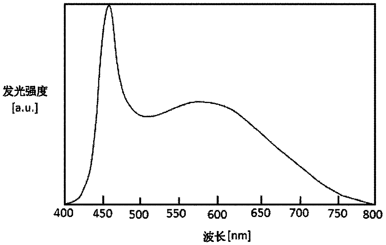
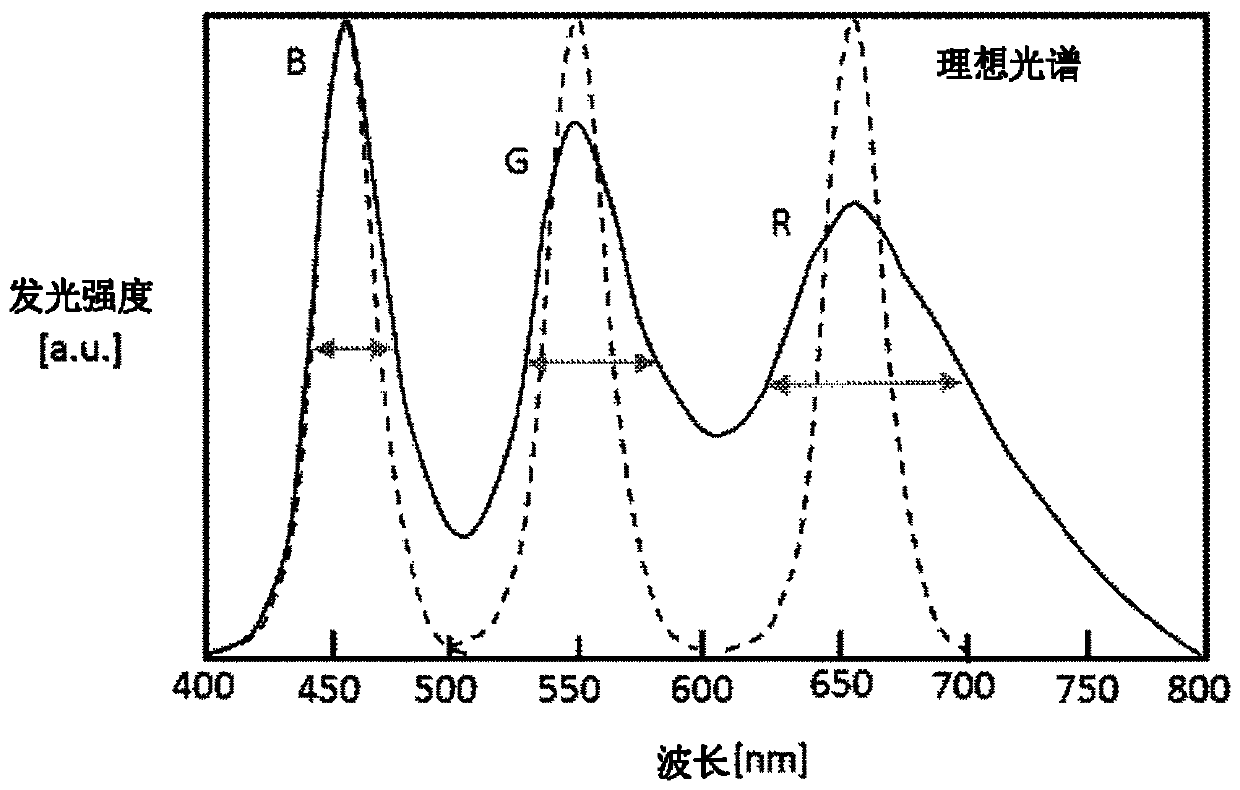
[0077] As mentioned above, such as Figure 18 As shown, in the present invention, a phosphor with an extremely sharp full width at half maximum can be obtained. Therefore, it is possible to obtain figure 2 The ideal RGB spectrum is documented. It can be seen that the present invention can provide such a highly efficient and stable semiconductor-type ph...


PUM

PropertyMeasurementUnit
thicknessaaaaaaaaaa
thicknessaaaaaaaaaa
thicknessaaaaaaaaaa

Abstract

The present invention is a semiconductor phosphor that emits photoluminescence when excitation light is injected. The semiconductor phosphor comprises at least one active layer made of a compound semiconductor and containing an n-type or p-type dopant and at least two barrier layers made of a compound semiconductor and having a band gap greater than that of the active layer. The semiconductor phosphor is characterized in that the active layer and the barrier layers are alternatingly stacked. On the above basis, provided is a semiconductor-type phosphor that facilitates wavelength adjustment, is highly efficient, and stable.

Description

technical field [0001] The present invention relates to a semiconductor-type phosphor for converting the wavelength of light, and more particularly, to a semiconductor-type phosphor for efficiently converting blue light into red. Background technique [0002] Generally, phosphors used in white LEDs include YAG-based and SiAlON (silicon-aluminum-oxynitride)-based phosphors. However, when converting the wavelength of blue light in the production of white LEDs, conventional phosphors always emit strong blue light ( figure 1 ). Nitride-based CASN and the like have been put to practical use as red phosphors, but there are problems in manufacturing RGB-type white LEDs due to their broad emission waveforms and difficulty in controlling wavelengths. In the manufacture of RGB-type white LEDs with high color rendering, it is advantageous to have a narrow emission spectrum of the phosphor. However, in the emission of general phosphors, the red spectrum is particularly broad, and ther...

Claims


Application Information

Patent Timeline
Patent Type & Authority Applications(China)
IPC IPC(8): C09K11/70
CPCC09K11/70C09K11/706C09K11/0883C30B25/183C30B29/40H01L33/00
Inventor 樋口晋酒井健滋山田雅人高桥雅宣石崎顺也
Owner SHIN-ETSU HANDOTAI CO LTD
Why Eureka
Try Eureka