Semiconductor phosphor
- Summary
- Abstract
- Description
- Claims
- Application Information
AI Technical Summary
Benefits of technology
Problems solved by technology
Method used
Image
Examples
example 1
[0060]Targeting the red region, an AlGaInP multilayer thin film shown in FIG. 14 was grown on a GaAs substrate by using an MOVPE apparatus according to the same procedure for common LED crystals. The layer for PL light emission was an MQW of GaInP (well layer) / AlInP (barrier layer), and the target wavelength was 635 [nm] at the peak wavelength. The dopant was Si with a carrier concentration of 3.5E17 [ / cm3]. Then, the GaAs substrate was removed by chemical etching because the target wavelength and equivalent wavelengths are absorbed otherwise. Subsequently, the grown multilayer thin film was bonded to a sapphire substrate with an adhesive agent. Thus, a semiconductor phosphor was obtained. The obtained semiconductor phosphor had a multiple quantum well structure which had 40 pairs of active layers each made of GaInP with a thickness of 5 nm and barrier layers each made of AlInP with a thickness 5 nm, and which was sandwiched by undoped cladding layers each made of AlInP with a thick...
example 2
[0064]Further, a semiconductor phosphor was prepared by the same method as in Example 1, except that the composition of the active layer was changed so as to emit light with a longer wavelength. The emission spectrum was measured. As a result, the half-value width was approximately 30 [nm] as shown in FIG. 19 and slightly increased in comparison with the semiconductor phosphor of Example 1, but the obtained emission spectrum was sharp at λp=660 [nm]. Thus, as a feature of the present invention, the wavelength can be changed exactly in the same manner as in ordinary LEDs.
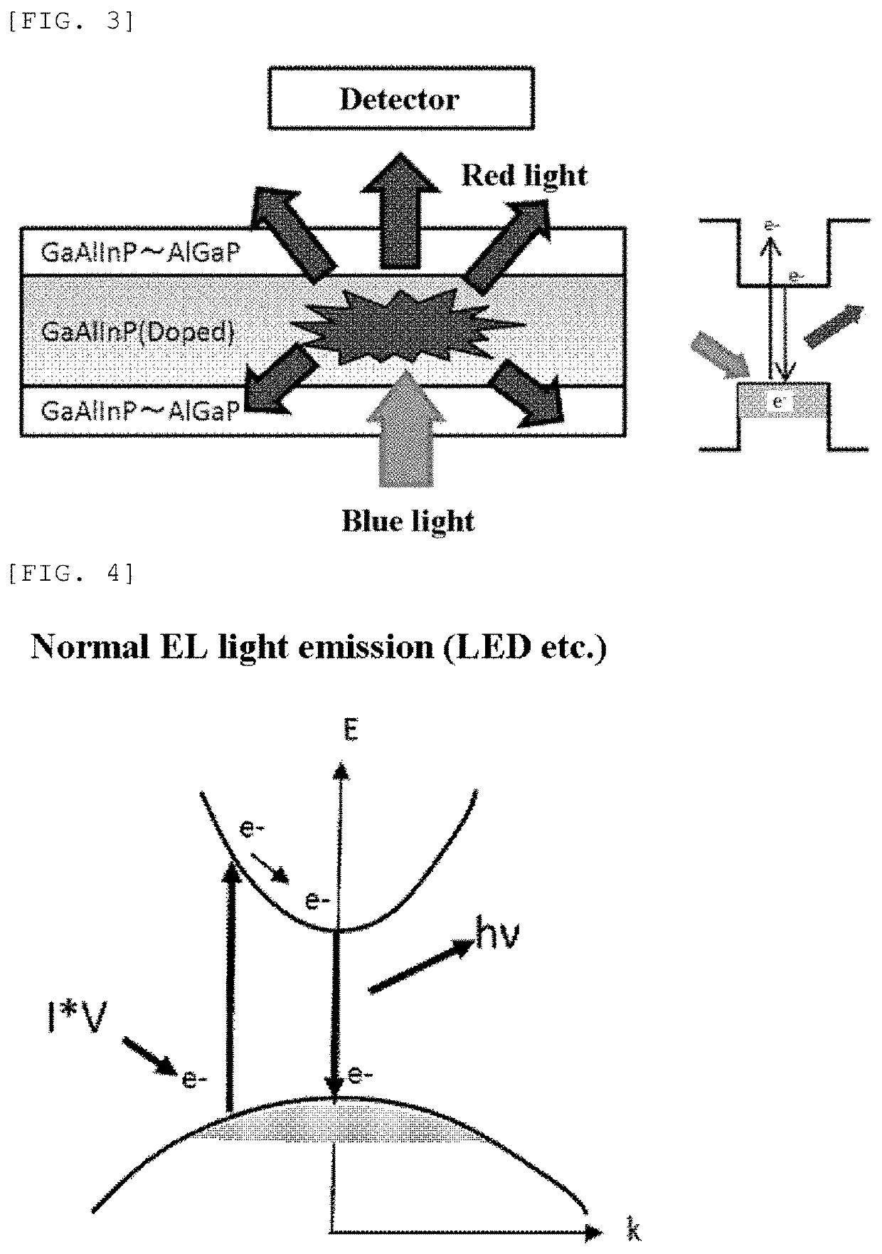
[0065]From the foregoing, according to the present invention, as shown in FIG. 18, the phosphor with quite a sharp half-value width was successfully obtained. Thus, the ideal RGB spectrums shown in FIG. 2 can be obtained. It has been revealed that the present invention makes is possible to provide a semiconductor phosphor which allows easy wavelength adjustment, high efficiency and stability.
PUM
 Abstract
Description
Claims
Application Information


