Check patentability & draft patents in minutes with Patsnap Eureka AI!

Synchronous semiconductor storage unit of reducing consumption current of input buffer circuit thereof

A technology of input buffering and buffering circuits, applied in static memory, digital memory information, information storage, etc., can solve problems such as hindering the realization of SDRAM, constant flow of differential amplification current, etc.

Inactive Publication Date: 2003-07-02
MITSUBISHI ELECTRIC CORP
View PDF2 Cites 1 Cited by
  • Summary
  • Abstract
  • Description
  • Claims
  • Application Information

AI Technical Summary

Problems solved by technology

Therefore, when the number of external signals increases due to the above-mentioned situation, the number of its input buffers will also increase accordingly, and if the differential amplifier circuit shown in Figure 19 is used in the input buffer of the first stage, the constant The current flowing through the differential amplification current will become large, which will hinder the realization of SDRAM with low current consumption

Method used


Image

  • Synchronous semiconductor storage unit of reducing consumption current of input buffer circuit thereof
  • Synchronous semiconductor storage unit of reducing consumption current of input buffer circuit thereof
  • Synchronous semiconductor storage unit of reducing consumption current of input buffer circuit thereof

Examples


Embodiment Construction

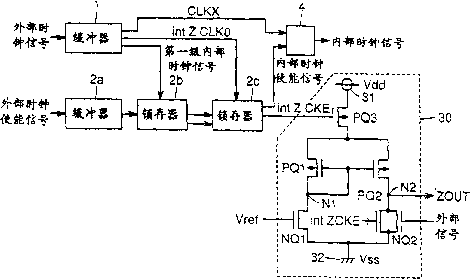
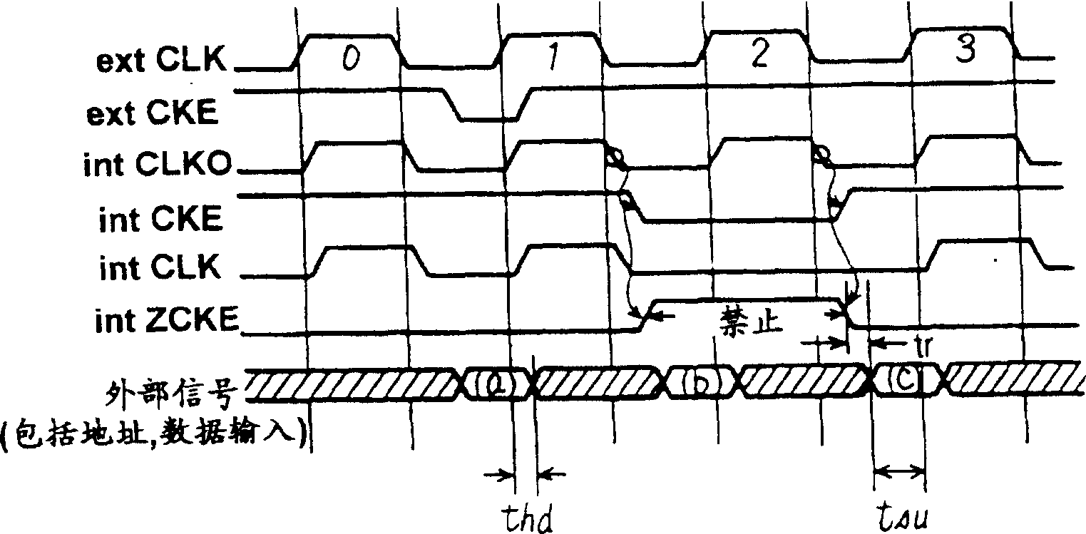
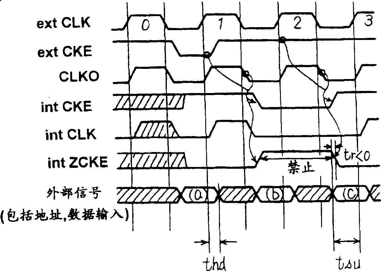
[0080] figure 1 The structure of the main part of an SDRAM which is the starting point of the present invention is shown. see figure 1 , the SDRAM includes a clock buffer circuit 1 and an internal clock generation circuit 4, wherein the clock buffer circuit buffers the external clock signal extCLK to generate an intermediate clock signal CLKX and first-level internal clock signals intCLK0 and intZCLK0; the internal clock generation circuit 4. Selectively activate according to the state of the internal clock enable signal intCKE, so as to generate the second-level internal clock signal intCLK from the intermediate clock signal CLKX. The structures of circuits 1 and 4 will be described in detail later. The internal clock signals intCLK0 and intZCLKO are generated by buffering the intermediate clock signal CLKX.

[0081] The SDRAM also includes a buffer circuit 2a, a first-stage latch circuit 2b, and a second-stage latch circuit 2c, wherein the buffer circuit 2a buffers the ex...


PUM


Abstract

An external clock enable signal is taken in accordance with a first internal clock signal from clock buffer circuit from which an input buffer enable signal is generated to be input to input buffer circuit. Current path in the input buffer circuit is shut off in accordance with the input buffer enable signal. Since the state of the input buffer enable signal is changed in synchronization with the rise of the internal clock signal, the set up time of the external signal can be sufficiently ensured while current consumption of input buffer circuit can be reduced.

Description

technical field [0001] The present invention relates to a clock synchronous type semiconductor memory device which operates synchronously with an external clock signal. More specifically, the present invention relates to the structure of an input buffer that accepts an external signal in a clock synchronization type semiconductor memory. Background technique [0002] In order to eliminate the difference in operating speed between a microprocessor and a memory, various memory LSIs capable of high-speed access have been proposed. These memory LSIs are characterized in that data input / output is performed synchronously with an external clock signal, thereby increasing the effective data transfer rate. One of such synchronous type semiconductor memories that operate synchronously with an external clock signal is Synchronous Dynamic Random Access Memory (hereinafter referred to as SDRAM). SDRAM includes some storage units, and generally each storage unit is a dynamic storage uni...

Claims


Application Information

Patent Timeline
IPC IPC(8): G11C11/413G11C7/10G11C11/407G11C11/408G11C11/409G11C11/4093G11C11/417
CPCG11C11/4082G11C7/1072G11C7/1093G11C7/1078G11C11/4093G11C11/401
Inventor 谷村政明小西康弘
Owner MITSUBISHI ELECTRIC CORP
Features
  • R&D
  • Intellectual Property
  • Life Sciences
  • Materials
  • Tech Scout
  • Unparalleled Data Quality
  • Higher Quality Content
  • 60% Fewer Hallucinations
Learn More