Optical device for metal surface polishing

A metal surface and optical device technology, applied in metal processing equipment, laser welding equipment, welding equipment, etc., can solve the problems of low polishing accuracy level and large temperature gradient, etc.

Active Publication Date: 2020-07-07
CHANGCHUN INST OF OPTICS FINE MECHANICS & PHYSICS CHINESE ACAD OF SCI
View PDF5 Cites 4 Cited by
  • Summary
  • Abstract
  • Description
  • Claims
  • Application Information

AI Technical Summary

Problems solved by technology

[0004] However, when long-pulse lasers are used to polish metal materials such as tungsten, more thermal effects will be generated on the surface of the material, resulting in a large temperature gradient of the material, which will generate greater thermal stress and pull the surface of the material to form cracks. This stress damage leads to polishing. The level of precision achieved is not high, and the surface roughness is usually on the order of microns
In addition, its polishing effect on metal is also affected by many factors, including laser wavelength, beam incident angle, laser scanning speed, scanning mode, etc., and how to accurately control various parameters to form a suitable thickness in a fixed area on the metal surface The molten metal layer still faces great challenges

Method used


Image

  • Optical device for metal surface polishing
  • Optical device for metal surface polishing
  • Optical device for metal surface polishing

Examples


Embodiment Construction

[0027] The following will clearly and completely describe the technical solutions in the embodiments of the present invention with reference to the accompanying drawings in the embodiments of the present invention. Obviously, the described embodiments are only some, not all, embodiments of the present invention. Based on the embodiments of the present invention, all other embodiments obtained by persons of ordinary skill in the art without making creative efforts belong to the protection scope of the present invention.

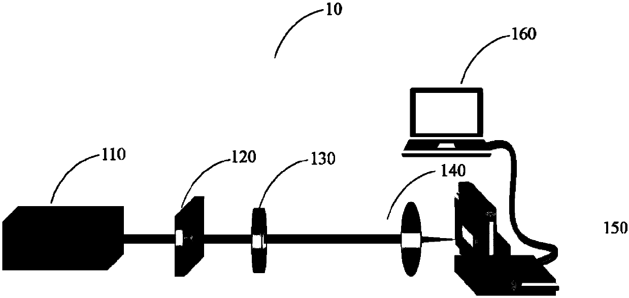
[0028] see figure 1 , is a structural schematic diagram of an optical device for metal surface polishing provided by an embodiment of the present invention, including a femtosecond laser light source 110, a yttrium vanadate birefringent crystal 120, an attenuation plate 130, a focusing objective lens 140, a three-dimensional mobile platform 150 and a control computer 160 , the metal to be polished is fixed on the three-dimensional mobile platform 150 , and the...


PUM

PropertyMeasurementUnit
diameteraaaaaaaaaa
lengthaaaaaaaaaa
lengthaaaaaaaaaa

Abstract

The invention provides an optical device for metal surface polishing. A laser beam emitted from a femtosecond laser light source passes through a yttrium vanadate birefringent crystal, an attenuationpipe and a focusing objective lens to be focused on a metal surface on a 3D mobile platform and conduct laser polishing treatment on the metal surface to obtain the smooth polished surface. The optical device for metal surface polishing, provided by the invention, realizes polishing on the metal surface by controlling related femtosecond laser machining parameters. Compared with an existing mechanical polishing method, one-time large-area quick polishing and micro-area polishing can be realized without abrasive paper, abrasive paste, chemical corrosive agents and other auxiliary materials. Moreover, the whole machining process is simple and easy to operate, the thermal effect can be neglected, and the high-precision polishing effect can be achieved. Meanwhile, through non-contact machining, damage, contamination and the like of stress to the surface of metal tungsten sample can be effectively avoided.

Description

technical field [0001] The invention relates to the technical field of optical processing, in particular to an optical device for polishing metal surfaces. Background technique [0002] As a refractory metal with high strength and high hardness, metal tungsten has good chemical stability and is not easy to be corroded. It has been widely used in electronics, light source, machinery industry and other departments. However, due to the high hardness of metal tungsten, when the traditional mechanical grinding and polishing method is used, the polishing cycle is long, the polishing accuracy is poor, the efficiency is low, and a variety of abrasives need to be added during the polishing process, so the price of polished metal tungsten products is generally higher. High, of which the polishing cost can account for more than half, while other more mature polishing methods, such as ion beam polishing, chemical polishing, electrolytic polishing, etc., usually require a strict process...

Claims


Application Information

Patent Timeline
Patent Type & Authority Applications(China)
IPC IPC(8): B23K26/352
Inventor 郑昕杨建军郭春雷
Owner CHANGCHUN INST OF OPTICS FINE MECHANICS & PHYSICS CHINESE ACAD OF SCI
Why Eureka
Try Eureka