MEMS packaging structure and manufacturing method thereof

A technology of a packaging structure and a manufacturing method, applied in the field of semiconductors, can solve the problems of shrinking the overall device, large differences in manufacturing processes, and complex processes.

Active Publication Date: 2020-07-07
NINGBO SEMICON INT CORP
View PDF16 Cites 10 Cited by
  • Summary
  • Abstract
  • Description
  • Claims
  • Application Information

AI Technical Summary

Problems solved by technology

[0003] However, for the MEMS device prepared by the above-mentioned former integration method, a pad area needs to be reserved on the packaging substrate, which usually has a large size, which is not conducive to the reduction of the overall device.
In addition, due to the large difference in the manufacturing process of MEMS chips with different functions (or structures), usually only MEMS chips with one function (or structure) can be produced on the same wafer, and it is difficult to use the latter integration method above on the same wafer. The semiconductor process is used to form MEMS chips with multiple functions on the wafer, and if the MEMS chip wafers with different functions are integrated on different control wafers for multiple times and then interconnected, the process is complicated and the cost is high, and the obtained MEMS Device size is still large
Therefore, the existing methods for integrating MEMS chips and the resulting MEMS packaging structures still cannot meet the requirements for size and functional integration capabilities in practical applications.

Method used


Image

  • MEMS packaging structure and manufacturing method thereof
  • MEMS packaging structure and manufacturing method thereof
  • MEMS packaging structure and manufacturing method thereof

Examples


Embodiment Construction

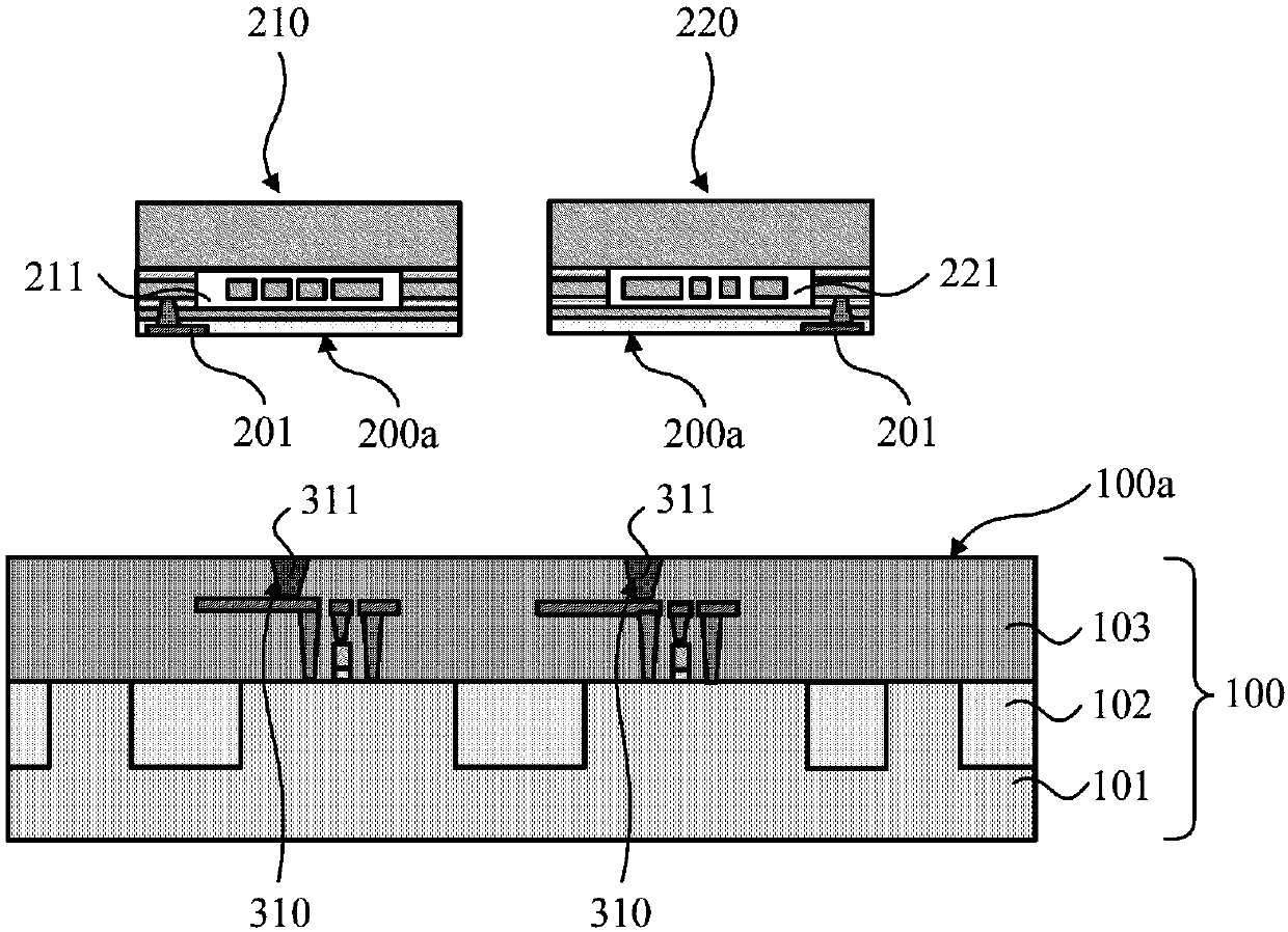
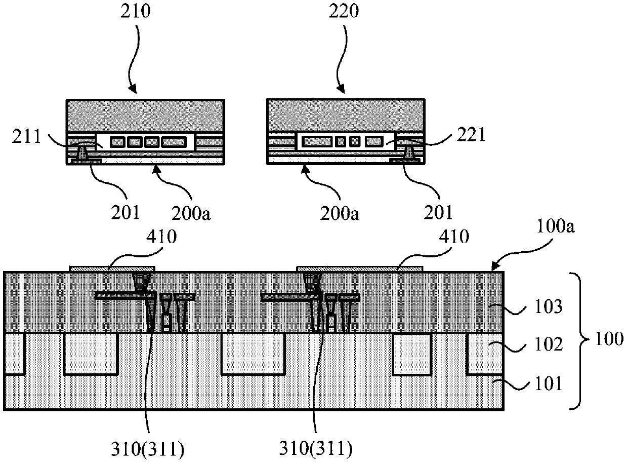
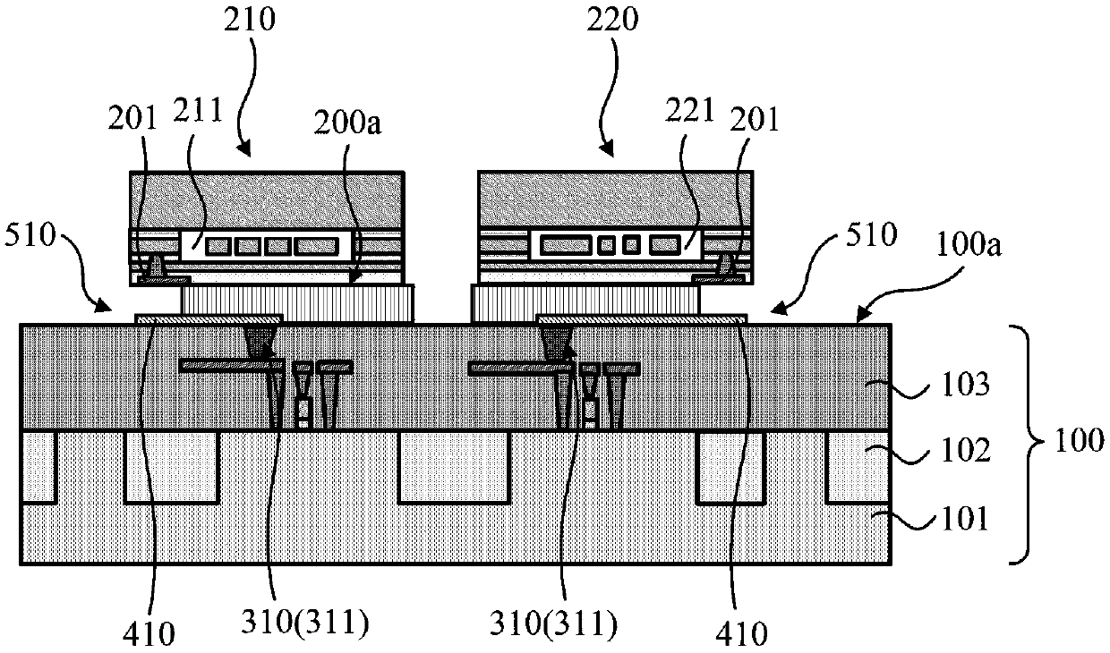
[0038] The MEMS packaging structure and its manufacturing method of the present invention will be further described in detail below in conjunction with the accompanying drawings and specific embodiments. The advantages and features of the present invention will become clearer from the following description. It should be noted that all the drawings are in a very simplified form and use imprecise scales, and are only used to facilitate and clearly assist the purpose of illustrating the embodiments of the present invention.

[0039] The terms "first", "second", etc. hereinafter are used to distinguish between similar elements, and are not necessarily used to describe a specific order or chronological order. It is to be understood that the terms so used are interchangeable under appropriate circumstances, for example, to enable the embodiments of the invention described herein to be operated in other sequences than described or illustrated herein. Similarly, if a method described...


PUM


Abstract

The invention provides an MEMS packaging structure and a manufacturing method thereof. The MEMS packaging structure comprises an MEMS chip and a device wafer, a control unit and an interconnection structure are arranged in the device wafer. A first contact pad is arranged on the first surface, the MEMS chip is provided with a closed micro-cavity, a second contact pad used for being connected withan external electric signal and a bonding surface, the MEMS chip is bonded to the first surface through a bonding layer, an opening is formed in the bonding layer, the first contact pad is electrically connected with the second contact pad, and the rewiring layer is arranged on the side opposite to the first surface. According to the MEMS packaging structure, the electrical interconnection of theMEMS chip and the device wafer is realized, the size can be reduced compared with the existing integration process, and the MEMS chips with the same or different structures and functions can be integrated on the same device wafer. The invention further provides a manufacturing method of the MEMS packaging structure.

Description

technical field [0001] The invention relates to the field of semiconductors, in particular to a MEMS packaging structure and a manufacturing method thereof. Background technique [0002] With the development trend of very large scale integrated circuits, the feature size of integrated circuits continues to decrease, and people's requirements for packaging technology of integrated circuits continue to increase accordingly. In the market for sensor-like MEMS packaging structures, microelectromechanical systems (MEMS) chips are widely used in product fields such as smartphones, fitness bracelets, printers, automobiles, drones, and VR / AR head-mounted devices. Commonly used MEMS chips include pressure sensors, accelerometers, gyroscopes, MEMS microphones, light sensors, catalytic sensors, and so on. MEMS chips are usually integrated with other chips by using a system in package (SIP) to form a MEMS device. Specifically, the MEMS chip is usually fabricated on one wafer, and the ...

Claims


Application Information

Patent Timeline
Patent Type & Authority Applications(China)
IPC IPC(8): B81B7/00B81C1/00
CPCB81B7/007B81C1/00301B81C2203/0154B81C1/0023B81B7/0006B81B7/02B81C1/00269B81C3/001B81B2207/07B81B2201/02B81B2201/03B81B2207/012B81B2207/096B81C2203/0792
Inventor 秦晓珊
Owner NINGBO SEMICON INT CORP
Why Eureka
Try Eureka