Micro-nano structure curing method

A curing method and technology of micro-nano structure, applied in the processing of photosensitive materials, etc., can solve the problems of inability to completely remove moisture, scrap wafers, and difficult to completely remove moisture from micro-nano pattern structures.

Inactive Publication Date: 2020-07-07
INST OF MICROELECTRONICS CHINESE ACAD OF SCI
View PDF3 Cites 0 Cited by
  • Summary
  • Abstract
  • Description
  • Claims
  • Application Information

AI Technical Summary

Problems solved by technology

[0004] Traditional drying methods, such as centrifugal drying, use centrifugal force to shake water out of the wafer to achieve drying. This method is effective for macroscopic structures, but it is difficult to completely remove the moisture attached to micro-nano pattern structures.
[0005] Another example is nitrogen purge, which uses the ejected nitrogen to purge the micro-nano structure on the wafer. This method is effective for wide and shallow groove structures, but it is basically ineffective for high-aspect-ratio photoresist deep grooves, and even There is also the possibility of blowing these structures down due to excessive blowing force
[0006] In addition, there are some composite drying methods, which increase the high-temperature drying process and use baking to dry. However, the water cannot be completely removed by drying or purging. The surface tension of the moisture inside will inevitably cause the micro-nano pattern to collapse from the inside, causing the entire wafer to be scrapped and the loss is great

Method used


Image

  • Micro-nano structure curing method

Examples


Embodiment Construction

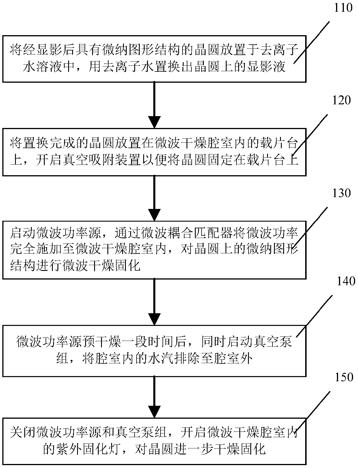
[0021] In order to better understand the above-mentioned technical solution, the above-mentioned technical solution will be described in detail below in conjunction with the accompanying drawings and specific implementation methods.

[0022] First, briefly describe the basic physical principle of drying using electromagnetic waves. Since water is a polar molecule, polar molecules do not show polarity when there is no external electromagnetic field. Under the condition of an external alternating electromagnetic field, the water molecules will be rapidly polarized, and the stronger the external alternating electromagnetic field, the stronger the polarization. At this time, the kinetic energy of the molecular thermal motion increases, that is, the heat increases, and the temperature of the water also increases, realizing the conversion of electromagnetic energy into heat energy. Therefore, water molecules can absorb electromagnetic waves and convert the energy of electromagnetic ...


PUM


Abstract

The invention provides a micro-nano structure curing method, which comprises the following steps: placing a developed wafer with a micro-nano pattern structure in a deionized water solution, and replacing a developing solution on the wafer with deionized water; placing the replaced wafer on a slide holder in a microwave drying chamber, and starting a vacuum adsorption device so as to fix the waferon the slide holder; starting a microwave power source, completely applying microwave power into the microwave drying chamber through a microwave coupling matcher, and performing microwave drying curing on the micro-nano pattern structure on the wafer; and after the microwave power source is started for a period of time, starting the vacuum pump set connected with the microwave drying chamber, sothat the water vapor in the chamber is discharged out of the chamber until solidification is completed, and finally moving out the wafer. According to the micro-nano solidification method, moisture on the wafer can be effectively and thoroughly removed, then the micro-nano structures are dried and solidified, and collapse of the micro-nano structures cannot be caused in the solidification process.

Description

technical field [0001] The invention relates to the technical field of semiconductor micro-nano structure manufacturing, in particular to a method for solidifying a micro-nano structure. Background technique [0002] Modern integrated circuit technology continues to develop towards smaller feature sizes and larger wafer sizes, such as feature sizes entering 10 nanometers and wafer diameters larger than 12 inches, which poses greater challenges to the manufacturing process of microelectronic devices. Because in the manufacturing process of microelectronic devices, with the further reduction of feature size and further increase of structural complexity, the collapse of micro-nano structures on the wafer has become an increasingly serious problem. There are many reasons for the structure to collapse, such as being subjected to external forces, the stress of the structure itself, weaker structural materials, and surface tension during the drying process. [0003] The general ma...

Claims


Application Information

Patent Timeline
Patent Type & Authority Applications(China)
IPC IPC(8): G03F7/40
CPCG03F7/40
Inventor 李勇滔景玉鹏
Owner INST OF MICROELECTRONICS CHINESE ACAD OF SCI
Why Eureka
Try Eureka