Chip package

A chip packaging and chip technology, applied in electrical components, electrical solid devices, circuits, etc., can solve the problems of increasing the PCBA processing process and the difficulty of QFN repair.

Pending Publication Date: 2020-07-07
ZTE CORP
View PDF8 Cites 1 Cited by
  • Summary
  • Abstract
  • Description
  • Claims
  • Application Information

AI Technical Summary

Problems solved by technology

Solution 1 is simple and effective, without increasing the existing production process, but now QFN is also developing towards high density, and many QFN devices have no space to increase pads or NC pads at the four corners
Solution 2 fixes the device and the PCB relatively. Even if stress is generated, it is difficult to act on the solder joints. Therefore, it is also very effective to solve the problem of QFN solder joint failure. However, dispensing increases the PCBA processing process, and after dispensing Difficulty in QFN rework

Method used


Image

  • Chip package
  • Chip package
  • Chip package

Examples


Embodiment 1

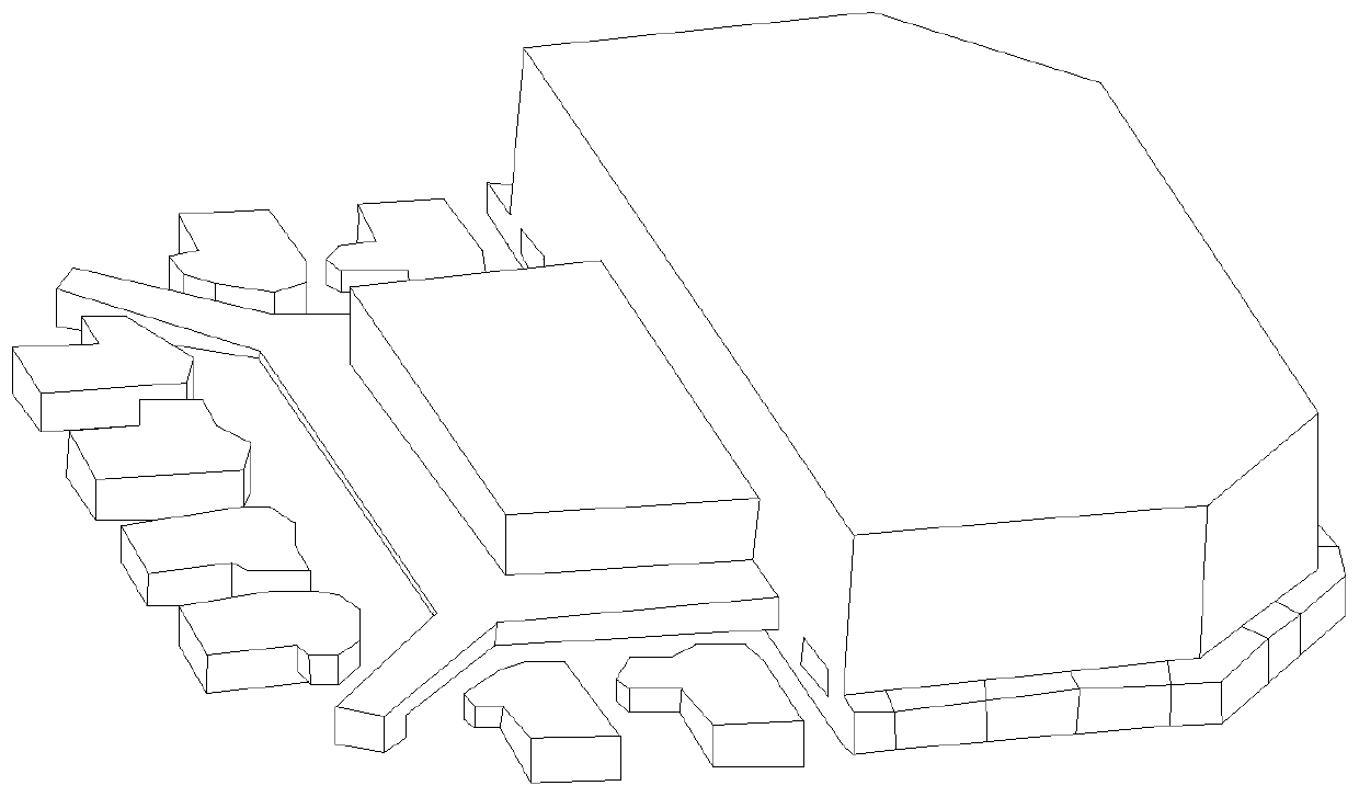
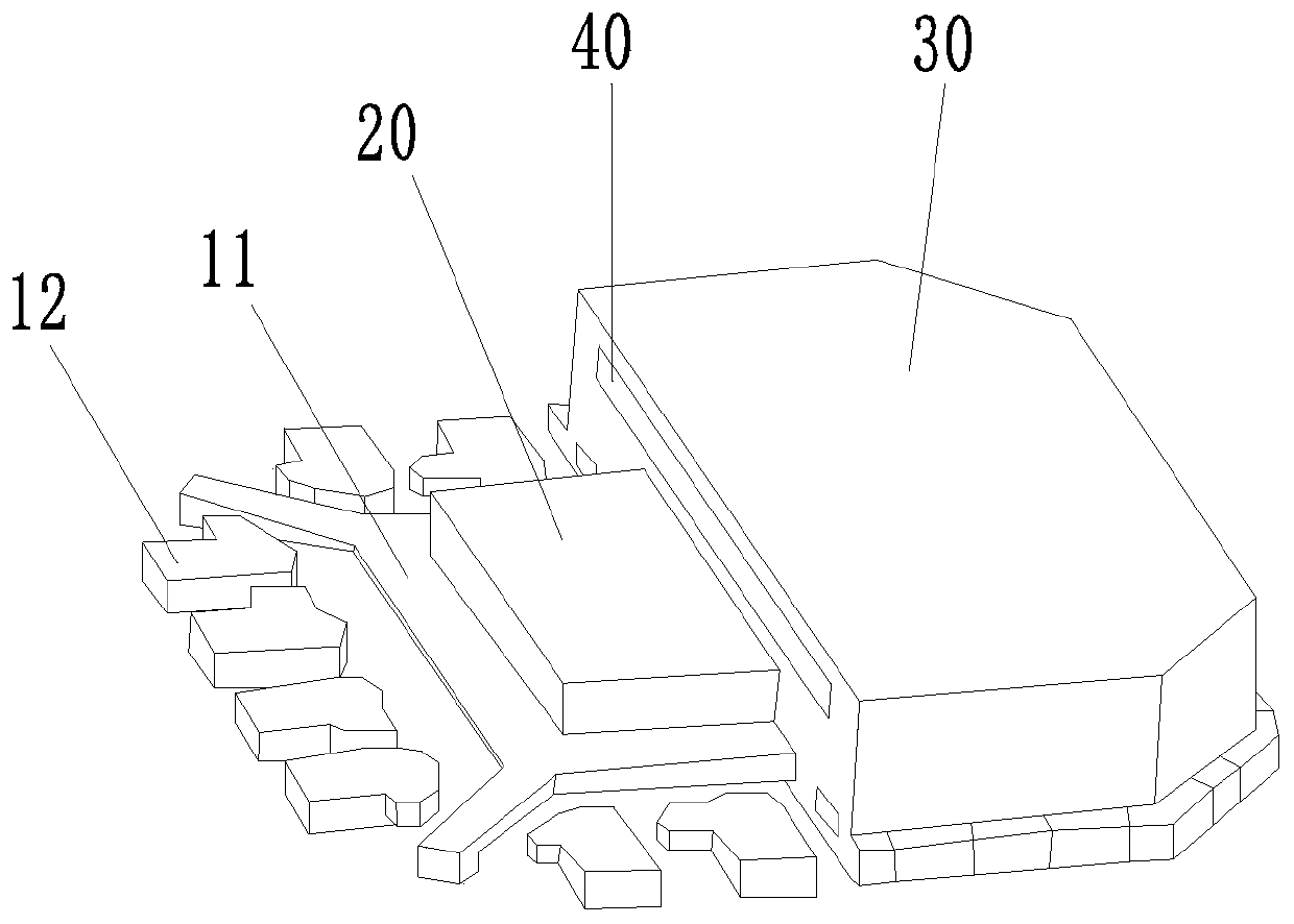
[0053] Such as image 3 As shown, a chip package is provided, including a pad 10, a chip 20, a package body 30 and a thermally deformable member 40, and the pad 10 includes a heat dissipation pad 11 and electrode contact pads arranged around the heat dissipation pad 11 12; the chip 20 is attached to the upper surface of the heat dissipation pad 11, and is electrically connected to the electrode contact pad 12; the package body 30 covers the sealing pad 10 and the chip 20, and the lower surface of the pad 10 is exposed to the package body 30 Surface; the thermally deformable member 40 is thermally deformed when heated, and is disposed on the package body 30 , and the thermally deformable member 40 and the bonding pad 10 are respectively disposed on two sides of the chip 20 .

[0054] In this example, if image 3 As shown, the thermally deformable member 40 is completely encapsulated inside the package body 30 . The chip 20 is selected as a silicon chip, which is connected to ...

Embodiment 2

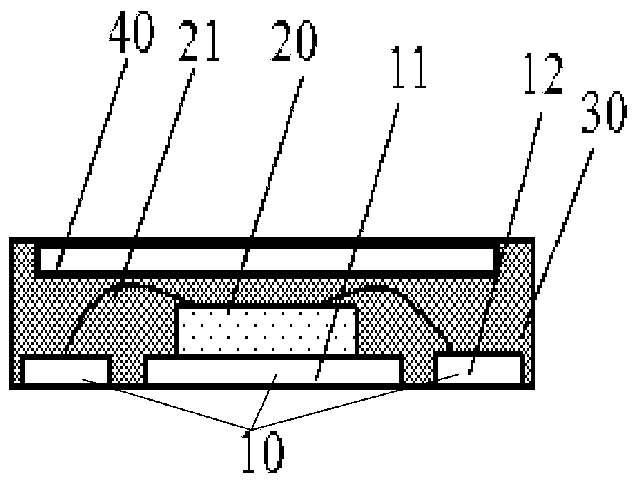
[0057] Such as Figure 4 As shown, a chip package is provided, including a pad 10, a chip 20, a package body 30 and a thermally deformable member 40, and the pad 10 includes a heat dissipation pad 11 and electrode contact pads arranged around the heat dissipation pad 11 12; the chip 20 is attached to the upper surface of the heat dissipation pad 11, and is electrically connected to the electrode contact pad 12; the package body 30 covers the sealing pad 10 and the chip 20, and the lower surface of the pad 10 is exposed to the package body 30 Surface; the thermally deformable member 40 is thermally deformed when heated, and is disposed on the package body 30 , and the thermally deformable member 40 and the bonding pad 10 are respectively disposed on two sides of the chip 20 .

[0058] In this example, if Figure 4 As shown, the thermally deformable member 40 of this embodiment is disposed outside the package body 30 . The chip 20 is selected as a silicon chip, which is connec...


PUM


Abstract

The invention relates to the technical field of component packaging, in particular to a chip package, which is a square flat leadless package. The chip package comprises: a bonding pad comprising a heat dissipation bonding pad and an electrode contact bonding pad arranged around the heat dissipation bonding pad; a chip which is attached to the upper surface of the heat dissipation bonding pad andis electrically connected with the electrode contact bonding pad; a packaging body which wraps the sealing bonding pad and the chip, wherein the lower surface of the bonding pad is exposed on the surface of the packaging body; and a thermal deformation component which can generate thermal deformation when being heated and is arranged on the packaging body, wherein the thermal deformation componentand the bonding pad are respectively arranged at two sides of the chip. The thermal deformation component has a stress correction effect on the thermal deformation of the device: when the thermal deformation component is heated, the thermal deformation component and the heat dissipation bonding pad are arranged up and down, so that the stress is offset or partially offset, and the deformation iseliminated or reduced. The device can avoid deformation caused by heating in the SMT assembly process or in long-term work, so that welding spots are protected, and the service life of the device is prolonged; and the layout area on the board is not occupied, the SMT process is not increased, and obvious advantages are achieved.

Description

technical field [0001] The invention relates to the technical field of component packaging, in particular to a chip packaging. Background technique [0002] Electronic products have always been evolving toward smaller size, lighter weight, faster speed, higher frequency, lower cost, and higher reliability. QFN devices are widely used in high-speed or microwave designs of 5G products due to their thinner thickness, leadless design, excellent heat dissipation performance, very low impedance and self-inductance. [0003] QFN is a leadless package with a square or rectangular shape. There is a large-area exposed pad at the center of the bottom of the package, which has a thermal conductivity. This pad is part of the internal thick copper frame structure, and QFN has excellent heat dissipation performance. s reason. However, this thick copper frame structure will undergo dynamic thermal deformation due to the influence of ambient temperature or power changes during SMT welding ...

Claims


Application Information

Patent Timeline
Patent Type & Authority Applications(China)
IPC IPC(8): H01L23/00
CPCH01L23/562H01L23/00
Inventor 赵丽贾忠中马军华王玉
Owner ZTE CORP
Why Eureka
Try Eureka