Preparation method of inspection sample of semiconductor device

A semiconductor and sample technology, applied in the field of TEM sample preparation, can solve the problem that there is no way to observe the cross-sectional structure of the semiconductor device to be tested, etc.

Pending Publication Date: 2020-07-10
SHANGHAI HUALI INTEGRATED CIRCUTE MFG CO LTD
View PDF8 Cites 2 Cited by
  • Summary
  • Abstract
  • Description
  • Claims
  • Application Information

AI Technical Summary

Problems solved by technology

Once such an ultra-thin flake TEM sample is prepared, it can and can only expose the cross-sectional structure of the semiconductor device to be tested in one direction, but there is no way to observe the cross-sectional structure of the same semiconductor device to be tested in another direction

Method used


Image

  • Preparation method of inspection sample of semiconductor device
  • Preparation method of inspection sample of semiconductor device
  • Preparation method of inspection sample of semiconductor device

Examples


Embodiment Construction

[0056] The present invention will be described in detail below in conjunction with the drawings and specific embodiments. Note that the following aspects described in conjunction with the drawings and specific embodiments are only exemplary, and should not be construed as limiting the protection scope of the present invention.

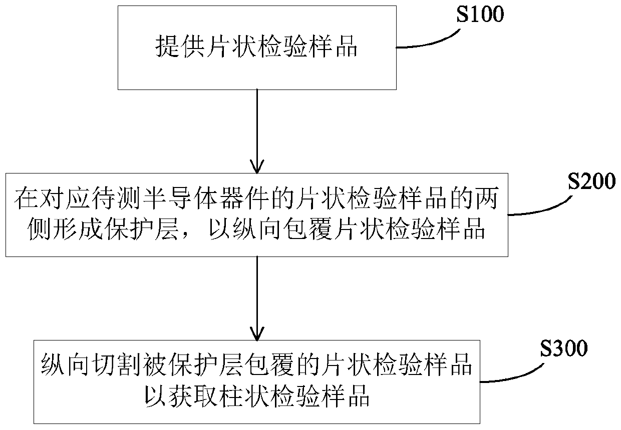
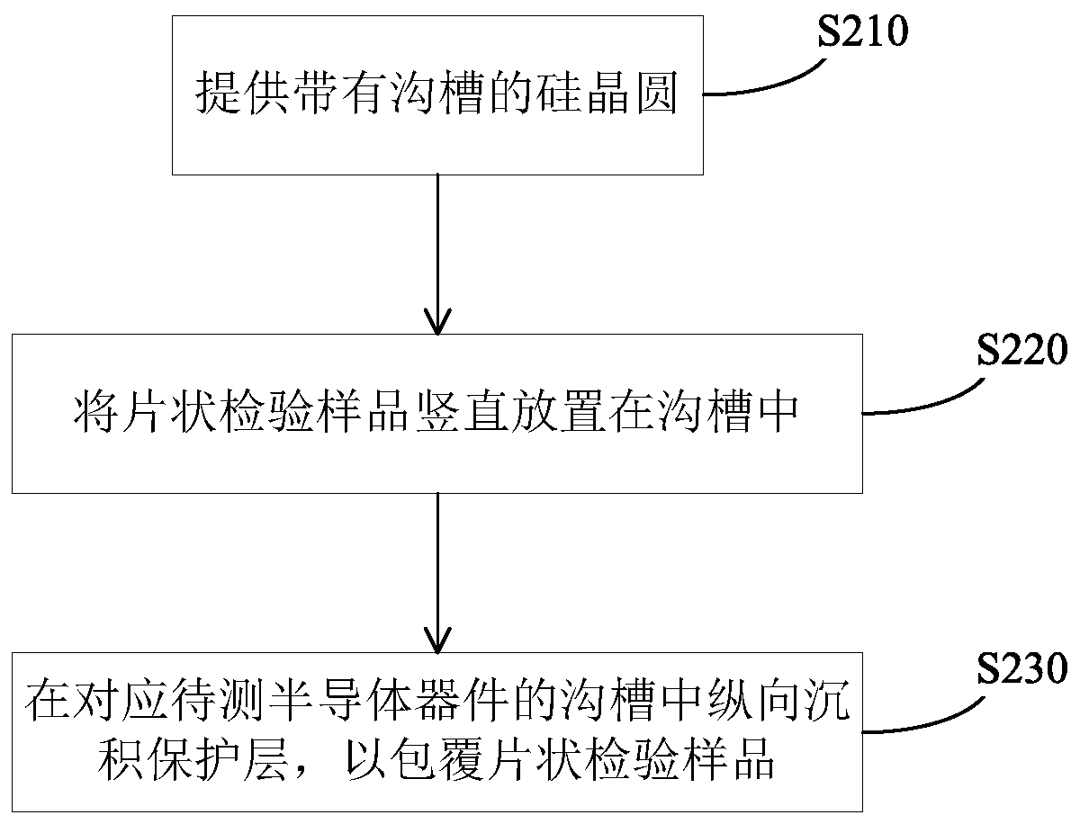
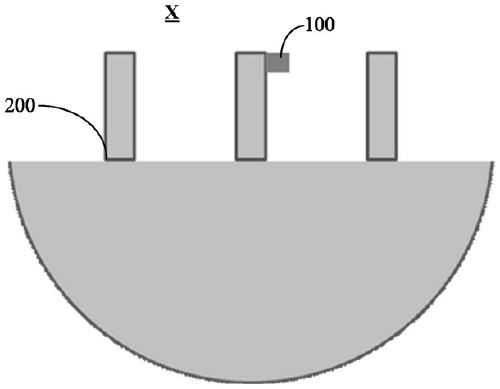
[0057] The invention relates to the testing field of semiconductor devices, and in particular to a method for preparing test samples of semiconductor devices. The method for preparing inspection samples of semiconductor devices provided by the present invention can perform ultra-thin sample preparation in two directions for the semiconductor device to be tested, so that the prepared inspection samples can be analyzed in two directions by using a transmission electron microscope. Obtain the structural information of the semiconductor device under test in two directions. It is of great help for the structural analysis of semiconductor devices with complex ...


PUM

PropertyMeasurementUnit
thicknessaaaaaaaaaa

Abstract

The invention provides a preparation method of an inspection sample of a semiconductor device, and the preparation method specifically comprises the following steps: providing a sheet-shaped inspection sample, and exposing a first to-be-detected cross section in the vertical direction of a to-be-detected semiconductor device on the observed transverse surface of the sheet-shaped inspection sample;forming protective layers on the two sides of the sheet-shaped test sample corresponding to the to-be-detected semiconductor device so as to longitudinally coat the sheet-shaped test sample; and longitudinally cutting the sheet-shaped test sample coated with the protective layers to obtain a columnar test sample, the observed longitudinal surface of the columnar test sample exposing a second to-be-tested cross section, perpendicular to the first to-be-tested cross section, of the to-be-tested semiconductor device in the vertical direction. According to the preparation method, accurate fixed-point and ultrathin sample preparation in two directions can be carried out on the same chip sample so that TEM analysis can be carried out on the to-be-detected sample in the two directions, and greathelp is provided for analysis of complex structures and complex defects.

Description

Technical field [0001] The invention relates to the field of semiconductors, and in particular to a method for preparing TEM samples in the field of semiconductor testing and analysis. Background technique [0002] Since the early years when Dr. Jack Kilby of Texas Instruments invented the integrated circuit, scientists and engineers have made numerous inventions and improvements in semiconductor devices and processes. The size of semiconductors has been significantly reduced in the past 50 years, which has led to ever-increasing processing speeds and ever-decreasing power consumption. So far, the development of semiconductors has roughly followed Moore's Law, which roughly means that the number of transistors in dense integrated circuits doubles approximately every two years. Now, the semiconductor process is moving towards below 20nm, some companies are working on 14nm process. Here is just a reference. The silicon atom is about 0.2nm, which means that the distance between tw...

Claims


Application Information

Patent Timeline
Patent Type & Authority Applications(China)
IPC IPC(8): G01N1/28G01Q30/20
CPCG01N1/28G01Q30/20G01N1/286G01N23/04G01N1/32
Inventor 陈强陈胜高金德
Owner SHANGHAI HUALI INTEGRATED CIRCUTE MFG CO LTD
Why Eureka
Try Eureka