A silicon carbide coaxial ultraviolet photodetector and its preparation method

A technology of electrical detectors and silicon carbide, applied in circuits, electrical components, semiconductor devices, etc., can solve the problems of reduced responsivity and quantum efficiency, achieve good device responsivity, improve efficiency, and broad application prospects

Active Publication Date: 2021-09-07
XIAMEN UNIV
View PDF7 Cites 0 Cited by
  • Summary
  • Abstract
  • Description
  • Claims
  • Application Information

AI Technical Summary

Problems solved by technology

[0004] The purpose of the present invention is to solve the shortcomings of the p+ layer in the silicon carbide ultraviolet photodetector with the conventional vertical sandwich p-i-n structure that the absorption of the ultraviolet incident signal leads to a decrease in responsivity and quantum efficiency, and provide a device that can improve the absorption of the incident light and the Carrier conversion, a silicon carbide coaxial ultraviolet photodetector and its preparation method for improving the detection ability of the detector

Method used


Image

  • A silicon carbide coaxial ultraviolet photodetector and its preparation method
  • A silicon carbide coaxial ultraviolet photodetector and its preparation method
  • A silicon carbide coaxial ultraviolet photodetector and its preparation method

Examples


preparation example Construction

[0035] The preparation method of the silicon carbide coaxial ultraviolet photodetector comprises the following steps:

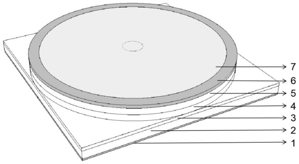
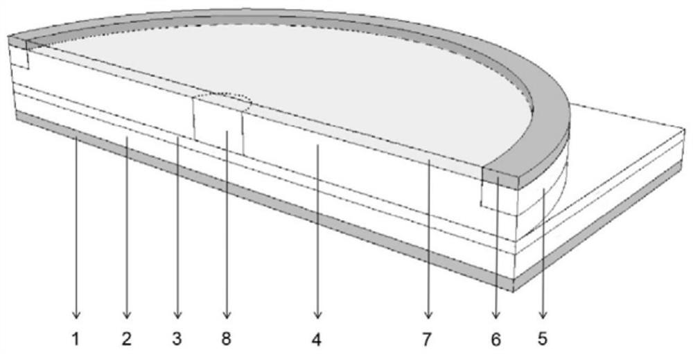
[0036] 1) RCA standard cleaning is performed on the silicon carbide n+ type substrate 2;

[0037] 2) Homoepitaxially grow a silicon carbide n-type buffer layer 3 and an unintentionally doped absorber layer on the Si surface of the silicon carbide n+ type substrate 2 after RCA standard cleaning; the doping of the silicon carbide n-type buffer layer 3 Concentration can be 1×10 18 / cm 3 ~5×10 18 / cm 3 , the thickness can be 100-300nm.

[0038] 3) Etching the sample to form a cylindrical unintentionally doped absorbing layer; the etching can use a coupled plasma etching method, and the order of doping concentration of the cylindrical unintentionally doped absorbing layer can be 10 13 / cm 3 ~10 14 / cm 3 .

[0039] 4) Ion implantation and annealing to prepare a cylindrical n-type layer in the center of the cylindrical non-intentionally doped absorber layer...


PUM

PropertyMeasurementUnit
radiusaaaaaaaaaa
radiusaaaaaaaaaa
heightaaaaaaaaaa

Abstract

A silicon carbide coaxial ultraviolet photodetector and a preparation method thereof relate to an ultraviolet photodetector. The silicon carbide coaxial ultraviolet photodetector is equipped with a silicon carbide n+ type substrate with a high doping concentration, a homogeneous n-type buffer layer is set on the silicon surface of the n+ type substrate, and a cylinder is set upward in the center of the n-type buffer layer Shaped silicon carbide n-type layer, with the axis of the n-type layer as the center, a cylindrical tubular silicon carbide low-doped i-type absorber layer and a cylindrical tubular silicon carbide p+-type ohmic contact layer are arranged in sequence, and the p+-type ohmic contact layers are all arranged on the i-type The upper part of the absorber layer is not in contact with the n+ type substrate, and the entire device forms a p-i-n structure from the outside to the inside in the horizontal direction. SiO 2 A passivation layer: an n+ type electrode is provided on the back of the n+ type substrate, and a p+ type electrode is provided on the upper surface of the p+ type ohmic contact layer side. Better device responsivity can be obtained, and the efficiency of collecting photogenerated carriers can be improved.

Description

technical field [0001] The invention relates to an ultraviolet photodetector, in particular to a silicon carbide coaxial ultraviolet photodetector capable of significantly improving the absorption and responsivity of ultraviolet solar-blind short-wave band signals and a preparation method thereof. Background technique [0002] As ultraviolet rays are more and more widely used in industrial manufacturing, medical sanitation and disinfection, and environmental monitoring, the detection technology of ultraviolet light band signals, especially ultraviolet light solar-blind band (wavelength 0.20-0.28μm) signals is gradually It has been paid attention to, and ultraviolet photodetectors of different materials and structures have been developed one after another. Among them, ultraviolet photodetectors of semiconductor materials have excellent characteristics such as low voltage, small size, and long life, which have become research hotspots. [0003] At present, the technology of si...

Claims


Application Information

Patent Timeline
Patent Type & Authority Patents(China)
IPC IPC(8): H01L31/105H01L31/0312H01L31/18
CPCH01L31/0312H01L31/105H01L31/1804Y02P70/50
Inventor 洪荣墩张锐军吴正云张峰蔡加法付钊林鼎渠
Owner XIAMEN UNIV
Why Eureka
Try Eureka