Rotary diffusion optical imaging system
An optical imaging system, a rotary technology, used in medical science, diagnosis using tomography, sensors, etc., can solve the problems of strict light-proof conditions, complex system structure, and high price.
Active Publication Date: 2020-07-31
XIDIAN UNIV
10 Cites 0 Cited by
AI-Extracted Technical Summary
Problems solved by technology
[0004] However, the structure of this system is too complicated. The light generated by the light source needs to pass through optical fibers, attenuators, and collimators to reach the imaging cavity. At the same time, the outgoing light signal also needs to pass through optical fibers, optical switches, collimators, and filter wheels to reach the detection chamber. device
In the whole process, the light passes through multiple devices, and it is inevitable that...
Method used
Please refer to Fig. 16, the rotary diffusion optical imaging system of the present embodiment uses laser diode as light source, replaces the light source system of traditional laser+collimator+attenuator+optical fiber; The multiplier tube and the drive circuit based on the flexible PCB replace the traditional optical fiber + optical switch + PMT acquisition system, and use the rotating table to drive the laser diode and silicon photomultiplier tube to rotate around the imaging cavity to obtain multiple position data, which can be obtained through the computer and Multi-channel high-speed acquisition card realizes multi-channel data acquisition. The rotating diffusion optical imaging system of this embodiment greatly simplifies the complexity of the original system. Because the laser diode and the silicon photomultiplier tube are close to the object to be measured, the light loss of the system can be reduced, and each channel is synchronized during acquisition, which improves the system efficiency. Acquisition speed realizes multi-channel synchronous acquisition. At the same time, since the laser diode can be added with high-frequency modulation, the sampling frequency of the acquisition card used in the rotary diffuse optical imaging system of the embodiment can reach 250M, so that the rotary diffuse optical imaging system of the embodiment can be used for frequency domain experiments.
The rotary diffusion optical imaging system of the present embodiment also includes a gain voltage module, and each detector has the same gain at the initial stage of design, that is, the output of the detectors for the same light source is consistent, but it is found in the measurement that there is the following phenomenon : The output values of the detector farthest from the light source and the nearest detector are quite different, resulting in the fact that when the detector farthest from the light sour...
Abstract
The invention discloses a rotary diffusion optical imaging system. The system comprises a light source unit, a detection unit, a bearing device with an imaging cavity, a rotatable sleeve device and adata acquisition unit, the light source unit comprises a plurality of light-emitting light sources, the detection unit comprises a plurality of detectors, the sleeve device comprises a sleeve, N rowsand M columns of through holes are formed in the sleeve, one light-emitting light source is correspondingly arranged in each through hole in the mth column, one detector is correspondingly arranged ineach through hole in columns except the mth column, and the sleeve sleeves the imaging cavity. According to the rotary diffusion optical imaging system provided by the invention, an optical fiber isno longer used for optical conduction, excitation and receiving are realized by adopting a mode that the light sources and the detectors are tightly attached to the measured object, the system complexity and the system cost are greatly reduced, meanwhile, the consistency of all channels and the signal to noise ratio of collected signals are improved, data collection and reconstruction are achieved, so that DOT imaging can be further studied, and the technology can be conveniently applied to mammary gland imaging.
Application Domain
Diagnostics using tomographySensors
Technology Topic
Signal-to-noise ratio (imaging)Engineering +7
Image
Examples
- Experimental program(1)
- Effect test(1)
Example Embodiment
[0059] Example one
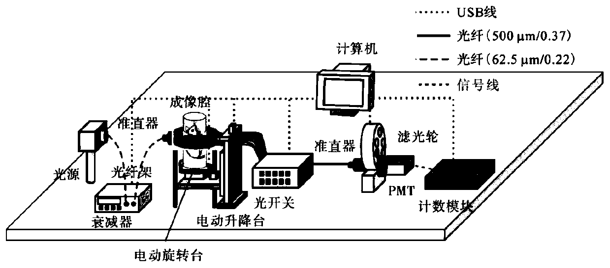
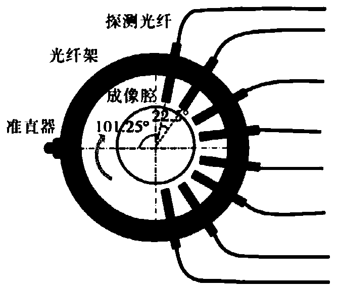
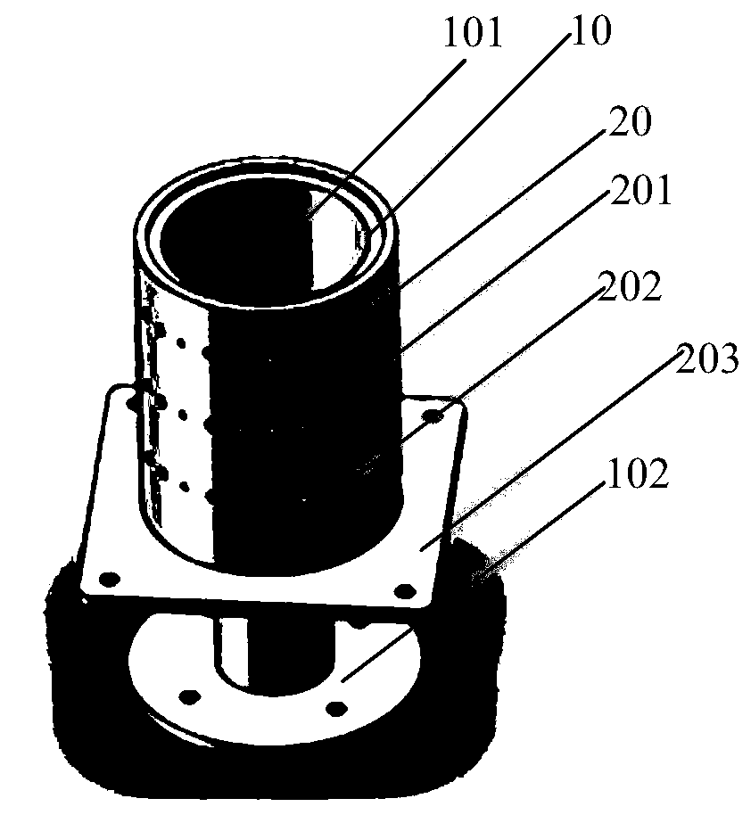
[0060] See image 3 , image 3 It is a schematic diagram of a rotating diffuse optical imaging system provided by an embodiment of the present invention. This embodiment provides a rotary diffusion optical imaging system. The rotary diffusion optical imaging system includes a light source unit, a detection unit, a carrying device 10 having an imaging cavity 101, a rotatable sleeve device 20, and a data acquisition unit, and the light source unit It includes several light sources, the detection unit includes several detectors. The sleeve device 20 includes a sleeve 201. The sleeve 201 is provided with N rows*M columns of through holes 202, and one corresponding to each through hole 202 in the mth column is provided. Luminous light source, a detector is provided in each through hole 202 except for the m-th column, and the sleeve 201 is sleeved with the imaging cavity 101, 1≤m≤M, wherein the light source unit is used to direct the imaging cavity 101 The measured object provides light signals in steady-state mode or frequency domain mode; the detection unit is used to detect light signals passing through the object to be measured and converts the light signals into electrical signals; the data acquisition unit is used to collect electrical signals and convert the electrical signals Convert to digital signal.
[0061] Preferably, the light-emitting source includes a laser diode, and the detector includes a silicon photomultiplier tube.
[0062] Generally, the diffusion optical imaging system can be divided into three modes: steady state, frequency domain and time domain. This embodiment mainly focuses on the steady state and frequency domain modes. The light source unit of this embodiment is used to provide illumination to the object to be measured (ie, breast ), the light source unit can provide the light signal in the steady-state mode or the frequency domain mode, and the detection unit can detect the light signal passing through the object to be measured, and the light signal Converted into electrical signals, the rotary diffusion optical imaging system of this embodiment further includes a bearing device 10, the bearing device 10 has an imaging cavity 101, and the imaging cavity 101 has a cavity in which certain optical parameters can be placed A connecting base 102 is also provided at the bottom end of the carrying device 10, and the connecting base 102 is used to fix the carrying device 10. For example, the connecting base 102 can be fixedly installed on the optical platform by means of bolts. When imaging the object to be measured, the connecting base 102 of the carrying device 10 can be fixed on an optical platform, and the object to be measured can be placed in the imaging cavity 101 containing the matching liquid; the rotating diffusion optical imaging of this embodiment The system also includes a rotatable sleeve device 20. The sleeve device 20 also includes a sleeve 201 that is sleeved on the outside of the imaging cavity 101. A base 203 is provided at the lower end of the sleeve device 20. The lower end of the base 203 can be connected to a rotating table, and the rotating table is connected to a motor that can drive the rotating table to rotate. When the sleeve device 20 is required to rotate, the rotating table can be driven to rotate by the motor to drive the sleeve device 20 to perform Spin.
[0063] In this embodiment, the sleeve 201 is provided with N rows*M columns of through holes 202, where N and M can be set according to actual needs, and N and M should be integers greater than 1, for example, N is 6, M is 24, two The distance of the through holes 202 between the rows is, for example, 15 mm, and the distance of the through holes 202 between the two columns is, for example, 13 mm. In this embodiment, each of the through holes 202 in the M column (for example, m columns) There is a laser diode corresponding to 202. The wavelength of the laser diode can be in the range of 600-900nm. This embodiment supports the access of high-frequency modulation signals of the laser diode, which can realize the control of the laser diode current, thereby being a rotary diffusion optical imaging system Provide a light source with adjustable light intensity suitable for both steady state and frequency domain dual modes. In addition, a silicon photomultiplier tube is provided in each through hole 202 except for the mth column. During imaging, the sleeve 201 rotates around the imaging cavity 101 by a certain angle each time, and then collects data once until the 360° measurement is completed. Data collection, for example, 17 positions can be collected for each collection in this rotating diffuse optical imaging system. In this embodiment, a silicon photomultiplier tube is used to form a detection array to realize the reception of light signals passing through the object to be measured and convert them into electrical signals. The silicon photomultiplier tube is a new type of photodetector device, which has the characteristics of strong adaptability, high gain, low cost, and good stability. This rotating diffusion optical imaging system works at the same time when all silicon photomultiplier tubes are used for data acquisition. The unit synchronously completes the data collection work. In order to enable the laser diode and the silicon photomultiplier tube to be closely attached to the sleeve 201, the laser diode, the silicon photomultiplier tube and related circuits can be integrated on a flexible PCB (Printed Circuit Board, printed circuit board). Because of its thin thickness and good plasticity, the designed detection unit has the characteristics of light weight and high plasticity, so that the laser diode, silicon photomultiplier tube and related circuits can be closely attached to the sleeve 201, compared to The rigid PCB reduces light loss, improves the signal-to-noise ratio and system imaging quality.
[0064] The rotary diffusion optical imaging system of this embodiment also includes a modulation signal generation unit, the modulation signal generation unit is connected to the light source unit, and the modulation signal generation unit is used to provide a modulation signal to the laser diode, see Image 6 , The modulation signal generation unit includes a DDS (Direct Digital Synthesis, direct digital frequency synthesis technology) module, a first signal generation module, a second signal generation module, a first signal output module, and a second signal output module, wherein,
[0065] DDS module, used to provide sinusoidal signals;
[0066] The first signal generation module, which is connected to the DDS module, is used to generate a first frequency signal or a DC signal by using a sinusoidal signal;
[0067] A second signal generating module, the first signal generating module is connected to the DDS module, and is configured to generate a second frequency signal using a sinusoidal signal, the frequency of the second frequency signal is greater than the frequency of the first frequency signal;
[0068] The first signal output module, connected to the first signal generation module, is used to output the DC signal of the first signal generation module, or convert the first frequency signal into a first square wave signal, and control the modulation depth and modulation depth of the first square wave signal size;
[0069] The second signal output module is connected to the second signal generation module, and is used for converting the second frequency signal into a second square wave signal and controlling the modulation depth and size of the second square wave signal.
[0070] That is, the first signal generation module can use the sine wave provided by the DDS module to generate the first frequency signal or DC signal, and the second signal generation module can use the sine wave provided by the DDS module to generate the second frequency signal, and the second frequency signal The frequency of the signal is greater than the first frequency signal, so the first frequency signal and the second frequency signal can be used to provide modulation signals of different frequencies, and the modulation signals of different frequencies can be used to achieve detection in the frequency domain mode, and the first signal generation module It can also generate a DC signal, so the steady-state mode can be detected under the DC signal. The first signal output module is used to convert the first frequency signal or DC signal into a first square wave signal, and use the first signal output module to control the modulation depth and size of the first square wave signal, that is, to modulate the first square wave signal. The peak size, maximum and minimum value of the wave signal, the second signal output module is used to convert the second frequency signal into a second square wave signal, and the second signal output module is used to control the modulation of the second square wave signal The depth and size are the peak size, maximum and minimum values of the modulated second square wave signal. For example, the frequency corresponding to the first frequency signal is 200 Hz, and the frequency corresponding to the second frequency signal is 30 MHz.
[0071] Preferably, the collection module is a collection card, for example, a multi-channel high-speed collection card.
[0072] Specifically, see Figure 7 , The first signal generating module includes resistor R1, resistor R3, transformer L1, capacitor C15, capacitor C16, capacitor C17, capacitor C18, capacitor C19, capacitor C20, capacitor C21, capacitor C22, capacitor C23, capacitor C24, capacitor C25, inductor L2, inductor L20, inductor L21, wherein pin 30 (pin CH0_IOUT) of the DDS module is connected to the first end of the resistor R1 and port 1 of the transformer L1, and pin 29 (pin CH0_IOUT) of the DDS module is connected to the resistor The first end of R3, the port 3 of the transformer L1, the second end of the resistor R1, and the second end of the resistor R3 are connected to the port 2 of the transformer L1 and the power end, the port 4 of the transformer L1 is connected to the ground end, and the port 6 of the transformer L1 is respectively Connect the first end of the capacitor C15, the first end of the capacitor C16, the first end of the capacitor C17 and the first end of the inductor L2. The second end of the capacitor C15 and the second end of the capacitor C16 are both connected to the ground end. The second end and the second end of the inductor L2 are both connected to the first end of the capacitor C18, the first end of the capacitor C19, the first end of the capacitor C20 and the first end of the inductor L20, the second end of the capacitor C18 and the first end of the capacitor C19 The second terminal is connected to the ground terminal, the second terminal of the capacitor C20 and the second terminal of the inductor L20 are both connected to the first terminal of the capacitor C21, the first terminal of the capacitor C22, the first terminal of the capacitor C23 and the first terminal of the inductor L21 , The second end of the capacitor C21 and the second end of the capacitor C22 are both connected to the ground, the second end of the capacitor C23 and the second end of the inductor L21 are both connected to the first end of the capacitor C24, the first end of the capacitor C25 and the first end The port V1, the second end of the capacitor C24, and the second end of the capacitor C25 are all connected to the ground terminal. Therefore, the first port V1 can output a first frequency signal or a DC signal.
[0073] Specifically, the first signal output module includes a first signal conversion module, a first amplification module, and a first signal output module, wherein the first signal conversion module, the first amplification module, and the first signal output module are connected in sequence, and the first signal The conversion module is used to convert the first frequency signal or the DC signal into a first square wave signal, the first amplifying module is used to amplify the first square wave signal, and the first signal output module is used to convert the amplified first square wave The signal is correspondingly output to the light source unit, among which, see Figure 8 , The first signal conversion module includes converter FB13, capacitor C66, capacitor C67, capacitor C68, resistor R23, sliding resistor R24, resistor R25, resistor R26, resistor R27, and resistor R28. The first end of converter FB13 is connected to the power supply terminal to convert The second end of the FB13 is connected to the first end of the capacitor C66, the first end of the capacitor C67, the first end of the resistor R23, the pin 1 (pin VCC) and the pin 8 (pin VDD) of the first chip, The second end of the capacitor C66 and the second end of the capacitor C67 are both connected to the ground, and the second end of the resistor R23 is connected to the sliding end of the resistor R24, the first end of the capacitor C68 and the pin 2 of the first chip (pin + IN ), the first end of the sliding resistor R24 is connected to the first end of the resistor R25, the second end of the resistor R25 and the second end of the capacitor C68 are connected to the ground, and the pin 3 (pin-IN) of the first chip is connected to the resistor R26 The second end of the resistor R26 is connected to the first port, the pin 4 (pin SHDN) of the first chip is connected to the first end of the resistor R27, and the second end of the resistor R27 is connected to the ground. Pin 5 (pin LE/HYST) is connected to the first end of resistor R28, the second end of resistor R28, pin 6 (pin VEE) of the first chip, and the second end of resistor R28 are connected to the ground end. Pin 7 (pin Q) of the chip is connected to the third port V3, and the model of the first chip is, for example, LTC6752-2. See Picture 9 , The first amplifying module includes capacitor C74, capacitor C75, capacitor C76, capacitor C77, capacitor C78, resistor R34, resistor R35, resistor R36, resistor R37, resistor R38, second chip, the first end of resistor R37 is connected to the first port V1, the second end of the resistor R37 is connected to the first end of the resistor R36 and the third port V3, the second end of the resistor R36 is connected to the pin 4 (pin Vin-) of the second chip, the first end of the resistor R38 and the capacitor The first end of C78, the second end of resistor R38 and the second end of capacitor C78 are connected to pin 1 (pin Vout) of the second chip and the fourth port V4, pin 2 of the second chip (pin-Vs) ) Connect the first end of the capacitor C76 and the first end of the capacitor C77, the second end of the capacitor C76 and the second end of the capacitor C77 are connected to the ground, and the pin 3 (pin Vin+) of the second chip is connected to the first end of the resistor R34 One end, the first end of the resistor R35, the second end of the resistor R34 is connected to the AO1 port, the AO1 port inputs the signal used to adjust the output signal strength, the second end of the resistor R35 is connected to the ground terminal, the pin 5 of the second chip (+Vs) is connected to the first terminal of the capacitor C74 and the first terminal of the capacitor C75, the second terminal of the capacitor C74 and the second terminal of the capacitor C75 are connected to the ground terminal, and the model of the second chip is OP_SOT23, for example. See Picture 10 , The first signal output module includes converter FB15, converter FB17, capacitor C81, capacitor C82, resistor R43, resistor R44, resistor R45, resistor R46, resistor 47, transistor U77, IPEX connector J28, and the first end of converter FB15 Connect the power terminal, the first terminal of the converter FB17 is connected to the power terminal, the second terminal of the converter FB15 and the second terminal of the converter FB17 are connected to the first terminal of the capacitor C81, the first terminal of the capacitor C82, and the first terminal of the resistor R43. The second end of the capacitor C81 and the second end of the capacitor C82 are connected to the ground terminal, the second end of the resistor R43 is connected to the collector of the transistor U77, the first end of the resistor R44 and the first end of the resistor R46 are connected to the fourth port V4 , The first end of the resistor R44 and the first end of the resistor R46 are also connected to the first end of the resistor R45, the second end of the resistor R44 is connected to the base of the transistor U77, the second end of the resistor R45 is connected to the AO2 port, and the AO2 port input A signal used to adjust the output signal strength. The second end of resistor R46 and the emitter of transistor U77 are connected to the first end of resistor R47. The second end of resistor R47 is connected to port 1 of IPEX connector J28, port 2 of IPEX connector J28 and Port 3 is connected to the ground terminal.
[0074] Specifically, please see again Figure 7 The second signal generation module includes resistor R4, resistor R5, transformer L6, capacitor C26, capacitor C27, capacitor C28, capacitor C29, capacitor C30, capacitor C31, capacitor C32, capacitor C33, capacitor C34, capacitor C35, capacitor C36, inductor L22, inductor L23, inductor L24, among them, pin 36 (pin CH1_IOUT) of the DDS module is connected to the first end of resistor R4 and port 1 of transformer L6, and pin 35 (pin CH1_IOUT) of the DDS module is connected to the resistor R5 The first end, the port 3 of the transformer L6, the second end of the resistor R4, and the second end of the resistor R5 are connected to the port 2 of the transformer L6 and the power end, the port 4 of the transformer L6 is connected to the ground terminal, and the port 6 of the transformer L6 is respectively connected to the capacitor The first end of C26, the first end of capacitor C27, the first end of capacitor C28 and the first end of inductor L22, the second end of capacitor C26 and the second end of capacitor C27 are all connected to ground, and the second end of capacitor C28 The terminal and the second terminal of the inductor L22 are both connected to the first terminal of the capacitor C29, the first terminal of the capacitor C30, the first terminal of the capacitor C31 and the first terminal of the inductor L23, the second terminal of the capacitor C29 and the second terminal of the capacitor C30 The second end of the capacitor C31 and the second end of the inductor L23 are both connected to the first end of the capacitor C32, the first end of the capacitor C33, the first end of the capacitor C34 and the first end of the inductor L24. The second terminal of C32 and the second terminal of capacitor C33 are both connected to the ground terminal. The second terminal of capacitor C34 and the second terminal of inductor L24 are both connected to the first terminal of capacitor C35, the first terminal of capacitor C36 and the second port V2. , The second terminal of the capacitor C35 and the second terminal of the capacitor C36 are both connected to the ground terminal. Therefore, the second port V2 can output the second frequency signal.
[0075] Specifically, the second signal output module includes a second signal conversion module, a second amplification module, and a second signal output module. The second signal conversion module, the second amplification module, and the second signal output module are connected in sequence, and the second signal The conversion module is used to convert the second frequency signal into a second square wave signal, the second amplifying module is used to amplify the second square wave signal, and the second signal output module is used to output the amplified second square wave signal. To the light source unit, where, see Picture 11 The second signal conversion module includes converter FB12, capacitor C63, capacitor C64, capacitor C65, sliding resistor R17, resistor R18, resistor R19, resistor R20, resistor R21, resistor R22, a third chip, and the first end of converter FB12 Connect the power terminal, the second terminal of the converter FB12 is connected to the first terminal of the capacitor C63, the first terminal of the capacitor C64, the first terminal of the resistor R18, the pin 1 (pin VCC) and pin 8 of the third chip ( Pin VDD), the second end of the capacitor C63 and the second end of the capacitor C64 are connected to the ground, the second end of the resistor R18 is connected to the sliding end of the resistor R17, the first end of the capacitor C65 and the pin 2 of the third chip (Pin + IN), the first end of the sliding resistor R17 is connected to the first end of the resistor R19, the second end of the resistor R19 and the second end of the capacitor C65 are connected to the ground, and the third chip's pin 3 (pin- IN) Connect the first end of the resistor R20, the second end of the resistor R20 is connected to the second port V2, the pin 4 (pin SHDN) of the third chip is connected to the first end of the resistor R21, and the second end of the resistor R21 is connected to ground Terminal, pin 5 (pin LE/HYST) of the third chip is connected to the first end of resistor R22, the second end of resistor R22, pin 6 (pin VEE) of the third chip and the second end of resistor R22 Connected to the ground, pin 7 (pin Q) of the third chip is connected to the fifth port V5, and the model of the SAN chip is, for example, LTC6752-2. See Picture 12 , The second amplifying module includes capacitor C69, capacitor C70, capacitor C71, capacitor C72, capacitor C73, resistor R29, resistor R30, resistor R31, resistor R32, resistor R33, and a fourth chip. The first end of resistor R32 is connected to the second port V2, the second end of the resistor R32 is connected to the first end of the resistor R31 and the fifth port V5, the second end of the resistor R31 is connected to the pin 4 (pin Vin-) of the fourth chip, the first end of the resistor R33 and the capacitor The first end of C73, the second end of resistor R33 and the second end of capacitor C73 are connected to pin 1 (pin Vout) of the fourth chip and the sixth port V6, pin 2 of the fourth chip (pin -Vs ) Connect the first end of the capacitor C71 and the first end of the capacitor C72, the second end of the capacitor C71 and the second end of the capacitor C72 are connected to the ground, and the pin 3 (pin Vin+) of the fourth chip is connected to the first end of the resistor R29 One end, the first end of the resistor R30, the second end of the resistor R30 is connected to the AO0 port, the AO0 port inputs the signal used to adjust the output signal strength, the second end of the resistor R29 is connected to the ground terminal, and the fourth chip pin 5 (+Vs) is connected to the first end of the capacitor C69 and the first end of the capacitor C70, the second end of the capacitor C69 and the second end of the capacitor C70 are connected to the ground terminal, and the model of the fourth chip is OP_SOT23, for example. See Figure 13 , The second signal output module includes converter FB14, converter FB16, capacitor C79, capacitor C80, resistor R39, resistor R40, resistor R41, resistor R42, transistor U5, IPEX connector J27, and the first end of converter FB14 is connected to the power supply terminal , The first end of converter FB16 is connected to the power source, the second end of converter FB14 and the second end of converter FB16 are connected to the first end of capacitor C79, the first end of capacitor C80, and the first end of resistor R39. The second end of C79 and the second end of capacitor C80 are connected to ground, the second end of resistor R39 is connected to the collector of transistor U5, the first end of resistor R40 and the first end of resistor R41 are connected to the sixth port V6, resistor R40 The second end of the resistor R41 is connected to the base of the transistor U5, the second end of the resistor R41 and the emitter of the transistor U5 are connected to the first end of the resistor R42, and the second end of the resistor R42 is connected to the port 1 of the IPEX connector J27 and the port of the IPEX connector J27 2 and port 3 are connected to the ground terminal.
[0076] See Figure 14a-14d The light source unit of this embodiment includes a strobe module, the strobe module includes a signal interface module, a number of light source communication modules, a light source strobe module, a control module, a resistor R49, an IPEX connector J29, and a light source strobe module includes a capacitor C83 and a capacitor C84 , Resistor R48, fifth chip, control module includes resistor R50, sixth chip, each light source connection module includes resistor R51, signal interface module is used to connect the first square wave signal or second square wave signal, light source connection module It is used to connect the corresponding laser diode. The light source strobe module is used to gate which laser diode to light up, and the control module is used to provide control signals to the light source connection module. Among them, port 2 and port 3 of IPEX connector J29 are connected to the ground terminal, IPEX Port 1 of connector J29 is connected to the first signal output module and the second signal output module. Specifically, port 1 of IPEX connector J29 is connected to port 1 of IPEX connector J27 and port 1 of IPEX connector J28. Port 1 of IPEX connector J29 is also connected to a resistor. The first end of R49 and the second end of resistor R49 are connected to the fifth port V5. The seventh port V7 is connected to the anodes of all laser diodes. The cathode of each laser diode is connected to the first end of a resistor R51 and the second end of resistor R51. Connect an eighth port, and all eighth ports correspond to the pins of the fifth chip. For example, the number of laser diodes is 6, such as Figure 14b with Figure 14c As shown, the six eighth ports are respectively connected to pin 1 (pin B4), pin 2 (pin B3), pin 3 (pin B2), and pin 4 (pin B1) of the fifth chip , Pin 14 (pin B6) and pin 15 (pin B5), pin 16 (pin VCC) of the fifth chip is connected to the first end of capacitor C83, the first end of capacitor C84, and the first end of capacitor C83 The second terminal, the second terminal of the capacitor C84 is connected to the ground terminal, the pin 5 of the fifth chip is connected to the first terminal of the resistor R48, the second terminal of the resistor R48 is connected to the ground terminal, and several control pins of the fifth chip are correspondingly connected to the sixth terminal. Several control pins of the chip, such as Figure 14c with 14d As shown, pin 7 (pin OE), pin 11 (pin S0), pin 10 (pin S1), and pin 9 (pin S2) of the fifth chip correspond to the pins of the sixth chip 6. Pin 7, Pin 8, Pin 9, Pin 5 of the sixth chip is connected to the first end of the resistor R50, and the second end of the resistor R50 is connected to the seventh port V7.
[0077] See Figure 15a-15e , The detection unit of this embodiment also includes a power supply access module, a gain voltage module, a number of detector connection modules, a number of amplification modules, and a number of detection output modules, where the power supply access module, the gain voltage module, and the detector connection module , The amplification module and the detection output module are connected in sequence, the power supply access module is connected with the power supply module to provide a power supply interface for the related circuit of the detection unit, the gain voltage module is used to provide the gain voltage to the silicon photomultiplier tube, and the detector connection module is used for Connected with the corresponding silicon photomultiplier tube, the amplification module is used to amplify the signal detected by the silicon photomultiplier tube, the detection output module is connected with the acquisition module, and is used to output the signal detected by the silicon photomultiplier tube to the acquisition module. , The power supply access module includes capacitor C85, capacitor C86, capacitor C87, capacitor C88, and the seventh chip. The gain voltage module includes capacitor C89, capacitor C90, capacitor C91, capacitor C92, capacitor C93, capacitor C94, resistor R52, resistor R53, Sliding resistor R54, eighth chip, detector connection module includes capacitor C95, capacitor C96, amplifying module includes capacitor C97, capacitor C98, capacitor C99, capacitor C100, capacitor C101, resistor 55, ninth chip, detection output module includes IPEX Connector J1, where the first end of the capacitor C85 and the first end of the capacitor C86 are connected to the power supply terminal, pins 1 and 2 of the seventh chip, and the second end of the capacitor C85 and the second end of the capacitor C86 are connected to the ground terminal , The first end of capacitor C87 is connected to pin 5 and pin 6 of the seventh chip, the second end of capacitor C87 is connected to ground, and the first end of capacitor C88 is connected to pin 7 and pin 8 of the seventh chip. The second terminal of C88 is connected to the ground terminal; the first terminal of capacitor C89, the first terminal of capacitor C90, the first terminal of capacitor C91, the first terminal of capacitor C85 and the first terminal of capacitor C86 are connected to the same power supply terminal. The first end of C89, the first end of capacitor C90, and the first end of capacitor C91 are also connected to pin 1 (pin IN), pin 2 (pin IN), and pin 3 (pin SHDN) of the eighth chip. ) And pin 9 (pin IN), the second end of the capacitor C89, the second end of the capacitor C90, and the second end of the capacitor C91 are connected to the ground, the first end of the capacitor C92, the first end of the capacitor C93, the capacitor The first end of C94 is connected to the power supply, pin 7 (pin OUT) and pin 8 (pin OUT) of the eighth chip, the first end of capacitor C92, the first end of capacitor C93, and the first end of capacitor C94. The terminal is also connected to the sliding terminal of the sliding resistor R54, the second terminal of the capacitor C92, the second terminal of the capacitor C93, and the second terminal of the capacitor C94 are connected to the ground terminal. The pin 6 (pin ADJ) of the eighth chip is connected to the resistor R52 The first end, the first end of the resistor R53, the second end of the resistor R52 is connected to the sliding resistor R54, and the second end of the resistor R53 is connected to the ground; pin 1 of each silicon photomultiplier tube is connected to the first end of a capacitor C95 And the first terminal of a capacitor C96, the first terminal of the capacitor C95 The first end of the capacitor C96 and the first end of the capacitor C92, the first end of the capacitor C93, and the first end of the capacitor C94 are connected to the same power supply terminal, and the second end of the capacitor C95 and the second end of the capacitor C96 are connected to the ground The pin 3 of the silicon photomultiplier tube is connected to the eighth port V8; each eighth port V8 is correspondingly connected to pin 4 (pin Vin-) of a ninth chip, the first end of the resistor 55, and the first end of the capacitor C101. At one end, the second end of the resistor 55 and the second end of the capacitor C101 are connected to pin 1 (pin VOUT) of the ninth chip and the ninth port V9, and the first end of the capacitor C97 and the first end of the capacitor C98 are connected to the Pin 5 (pin +Vs) of the nine-chip, the second end of the capacitor C97 and the second end of the capacitor C98 are connected to the ground, and the first end of the capacitor C99 and the first end of the capacitor C100 are connected to the pin of the ninth chip 2(Pin-Vs), the second end of capacitor C99 and the second end of capacitor C100 are connected to the ground terminal, each ninth port is connected to port 1 of an IPEX connector J1, and port 2 of IPEX connector J1 is connected to port 3 Ground terminal, the acquisition module can be connected to IPEX connector J1 through the IPEX interface.
PUM


Description & Claims & Application Information
We can also present the details of the Description, Claims and Application information to help users get a comprehensive understanding of the technical details of the patent, such as background art, summary of invention, brief description of drawings, description of embodiments, and other original content. On the other hand, users can also determine the specific scope of protection of the technology through the list of claims; as well as understand the changes in the life cycle of the technology with the presentation of the patent timeline. Login to view more.